 63
63
PowerColor Radeon RX 7900 GRE Hellhound Review
(63 Comments) »Introduction
PowerColor Radeon RX 7900 GRE Hellhound is the company's second premium custom-design implementation of the RX 7900 GRE, positioned a notch behind the company's Red Devil flagship. The Radeon RX 7900 GRE (Golden Rabbit Edition) started out as a China-exclusive limited edition product to mark the Year of the Rabbit, but found itself growing in importance to AMD in January 2024, with NVIDIA's brisk launches of the GeForce RTX 4070 SUPER. The Radeon RX 7800 XT beats the original RTX 4070 in raster gaming workloads, but NVIDIA plugged this gap with the RTX 4070 SUPER. The RX 7900 GRE had been around since Summer 2023, and so it was a matter of simply pricing it right for the global market, and giving it a wider launch outside China.

There is an interesting story behind the RX 7900 GRE. AMD had designed a compacted version of the Navi 31 package to drive the mobile versions of the RX 7900 series. This package is rumored to be pin-compatible with the Navi 32 package that powers the RX 7800 XT, allowing AMD's add-in board partners to reuse their RX 7800-series PCBs with compacted Navi 31. This package only has pins for a 256-bit memory bus even though the Navi 31 chip is capable of 384-bit, and so the RX 7900 GRE gets 16 GB of GDDR6 memory across this 256-bit memory bus. With the RX 7900 GRE having a similar 260 W total board power to the RX 7800 XT and its 265 W, AMD gets to minimize the R&D costs for its partners by not only letting them reuse the RX 7800 XT PCB, but also carry over cooling solutions from their RX 7800 XT products.
Navi 31 is a chiplet-based GPU. AMD identified components on the GPU that tangibly benefit from the switch to the newer 5 nm EUV foundry node—basically the GPU's front-end and shader engines, or all its logic-heavy components; and clumped them into a large central chiplet called the graphics compute die (GCD). All the memory-heavy components that don't benefit as much from 5 nm, namely the memory controllers and the Infinity Cache, have been disaggregated to smaller chiplets called the memory cache dies (MCDs), built on the older 6 nm process. Each MCD has a 16 MB segment of the Infinity Cache, and a 64-bit portion of the memory bus. There are six of these on the Navi 31 (96 MB cache, 384-bit memory bus), and four on the Navi 32 (64 MB cache, 256-bit memory bus). On the RX 7900 GRE, AMD enabled four of these MCDs.
The RX 7900 GRE has been carved out of the Navi 31 silicon by not just disabling two of its six MCDs, but also enabling just 80 out of the 96 compute units, for 5,120 stream processors, 160 AI accelerators, 80 Ray accelerators, 320 TMUs, and 160 out of the 192 available ROPs. The GPU is clocked at 1880 MHz Game clock, which PowerColor has further overclocked; while the memory, interestingly, ticks at 18 Gbps, which is slower than the 19.5 Gbps of the RX 7800 XT. At 18 Gbps, the GPU enjoys 576 GB/s of bandwidth.
The underlying graphics architecture is AMD's latest RDNA 3, which the company engineered to take advantage of the 5 nm process. The new dual instruction issue rate compute unit comes with a 17% IPC increase over the RDNA 2 compute unit, and supports newer AI-relevant instructions. The AI accelerator prepares matrix math for execution on the stream processors, providing a large speedup in AI DNN building and training. The 2nd generation Ray accelerator comes with a 50% improvement in ray intersection performance. The new multi-draw indirect accelerator (MDIA) is an exotic new on-silicon accelerator that can significantly speed up Direct3D 12 workloads that use MDI instructions.
The PowerColor RX 7900 GRE Hellhound looks very similar to the company's RX 7800 XT GRE, as it's mostly reusing the board design. The large aluminium fin-stack heatsink uses a trio of LED illuminated fans, while enthusiasts can benefit from features such as dual-BIOS. The card comes with a healthy factory overclock of 2013 MHz Game clock (vs. 1880 MHz reference), while leaving the memory speed untouched. PowerColor is pricing the RX 7900 GRE at $580, a slight premium over the $550 AMD baseline.
Short 10-Minute Video Summary Comparing 6x RX 7900 GRE
Our goal with the videos is to create short summaries, not go into all the details and test results, which can be found in this written review.
| Price | Cores | ROPs | Core Clock | Boost Clock | Memory Clock | GPU | Transistors | Memory | |
|---|---|---|---|---|---|---|---|---|---|
| RTX 3070 | $310 | 5888 | 96 | 1500 MHz | 1725 MHz | 1750 MHz | GA104 | 17400M | 8 GB, GDDR6, 256-bit |
| RTX 3070 Ti | $350 | 6144 | 96 | 1575 MHz | 1770 MHz | 1188 MHz | GA104 | 17400M | 8 GB, GDDR6X, 256-bit |
| RX 6800 | $450 | 3840 | 96 | 1815 MHz | 2105 MHz | 2000 MHz | Navi 21 | 26800M | 16 GB, GDDR6, 256-bit |
| RX 7700 XT | $430 | 3456 | 96 | 2171 MHz | 2544 MHz | 2250 MHz | Navi 32 | 26500M | 12 GB, GDDR6, 192-bit |
| RX 6800 XT | $500 | 4608 | 128 | 2015 MHz | 2250 MHz | 2000 MHz | Navi 21 | 26800M | 16 GB, GDDR6, 256-bit |
| RTX 3080 | $450 | 8704 | 96 | 1440 MHz | 1710 MHz | 1188 MHz | GA102 | 28000M | 10 GB, GDDR6X, 320-bit |
| RTX 4070 | $525 | 5888 | 64 | 1920 MHz | 2475 MHz | 1313 MHz | AD104 | 35800M | 12 GB, GDDR6X, 192-bit |
| RX 7800 XT | $500 | 3840 | 96 | 2124 MHz | 2430 MHz | 2425 MHz | Navi 32 | 28100M | 16 GB, GDDR6, 256-bit |
| RX 6900 XT | $650 | 5120 | 128 | 2015 MHz | 2250 MHz | 2000 MHz | Navi 21 | 26800M | 16 GB, GDDR6, 256-bit |
| RX 6950 XT | $630 | 5120 | 128 | 2100 MHz | 2310 MHz | 2250 MHz | Navi 21 | 26800M | 16 GB, GDDR6, 256-bit |
| RTX 3090 | $800 | 10496 | 112 | 1395 MHz | 1695 MHz | 1219 MHz | GA102 | 28000M | 24 GB, GDDR6X, 384-bit |
| RTX 4070 Super | $590 | 7168 | 80 | 1980 MHz | 2475 MHz | 1313 MHz | AD104 | 35800M | 12 GB, GDDR6X, 192-bit |
| RX 7900 GRE | $550 | 5120 | 160 | 1880 MHz | 2245 MHz | 2250 MHz | Navi 31 | 57700M | 16 GB, GDDR6, 256-bit |
| PowerColor RX 7900 GRE Hellhound | $580 | 5120 | 160 | 2013 MHz | 2366 MHz | 2250 MHz | Navi 31 | 57700M | 16 GB, GDDR6, 256-bit |
| RTX 4070 Ti | $720 | 7680 | 80 | 2310 MHz | 2610 MHz | 1313 MHz | AD104 | 35800M | 12 GB, GDDR6X, 192-bit |
| RTX 4070 Ti Super | $800 | 8448 | 112 | 2340 MHz | 2610 MHz | 1313 MHz | AD103 | 45900M | 16 GB, GDDR6X, 256-bit |
| RX 7900 XT | $700 | 5376 | 192 | 2000 MHz | 2400 MHz | 2500 MHz | Navi 31 | 57700M | 20 GB, GDDR6, 320-bit |
| RTX 3090 Ti | $1050 | 10752 | 112 | 1560 MHz | 1950 MHz | 1313 MHz | GA102 | 28000M | 24 GB, GDDR6X, 384-bit |
| RTX 4080 | $1200 | 9728 | 112 | 2205 MHz | 2505 MHz | 1400 MHz | AD103 | 45900M | 16 GB, GDDR6X, 256-bit |
| RTX 4080 Super | $1300 | 10240 | 112 | 2295 MHz | 2550 MHz | 1438 MHz | AD103 | 45900M | 16 GB, GDDR6X, 256-bit |
| RX 7900 XTX | $910 | 6144 | 192 | 2300 MHz | 2500 MHz | 2500 MHz | Navi 31 | 57700M | 24 GB, GDDR6, 384-bit |
| RTX 4090 | $1850 | 16384 | 176 | 2235 MHz | 2520 MHz | 1313 MHz | AD102 | 76300M | 24 GB, GDDR6X, 384-bit |
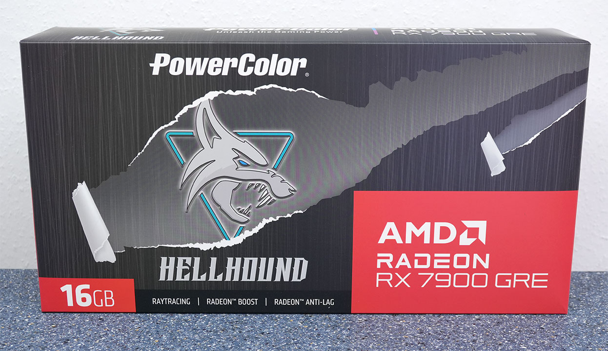
Packaging

The Card


The PowerColor HellHound uses a mostly-black color theme, with some silvery highlights around the fans, paired with transparent fan blades. Both the cooler shroud and backplate are made from metal.


Dimensions of the card are 32.0 x 13.0 cm, and it weighs 1260 g.


Installation requires three slots in your system.

Display connectivity includes three standard DisplayPort 2.1 ports (RDNA 2 had 1.4a) and one HDMI 2.1a (same as RDNA 2).
AMD has upgraded their encode/decode setup. It now comes with two independent hardware units that can encode and decode two streams of video in parallel, or one stream at double the FPS rate. There's support for VP9, H.264, H.265 and AV1 decode, and encoding is supported for H.264, H.265 and AV1.

The card uses a classic dual 8-pin plus PCIe slot power input config, rated for 375 W maximum power. NVIDIA on the other hand uses the new 12+4 pin ATX 12V-2x6 connector, which is rated for up to 600 W of power draw. Right next to the power inputs, there's a physical switch that lets you shut off the RGB lighting—without any software installation required.


The card comes with fixed-color lighting on the front and back, which can be changed between blue and purple, or turned off.

PowerColor has equipped their Hellhound with a dual BIOS feature, the second BIOS lets you enable a "quiet" mode that runs the fans at reduced fan speed for improved acoustics.
Teardown


The main heatsink uses five heatpipes. It also provides cooling for the memory chips and VRM circuitry.


The backplate is made of metal and protects the card against damage during installation and handling.
High-resolution PCB Pictures
These pictures are for the convenience of volt modders and people who would like to see all the finer details on the PCB. Feel free to link back to us and use these in your articles, videos or forum posts.

High-resolution versions are also available (front, back).
Circuit Board (PCB) Analysis
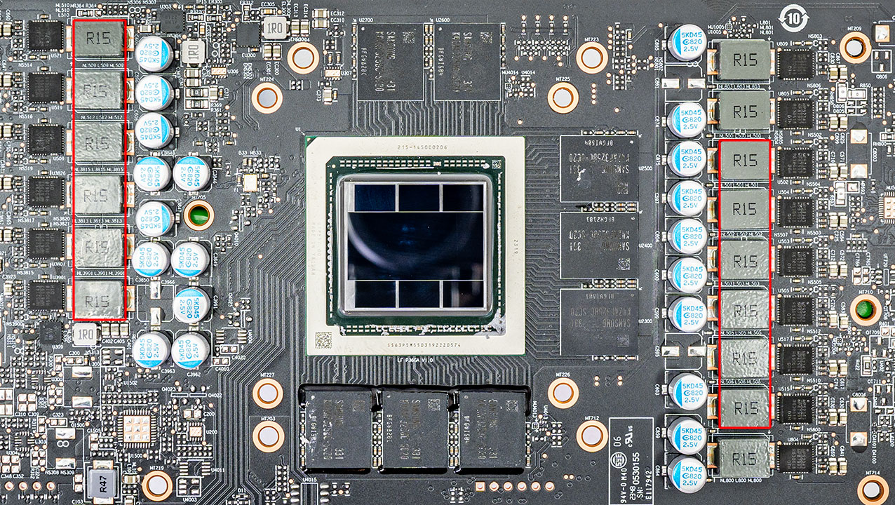

GPU voltage is a 12-phase design, managed by a Monolithic Power Systems MP2857 controller.

Monolithic MP87997 DrMOS components are used for GPU voltage; they are rated for 70 A of current each.

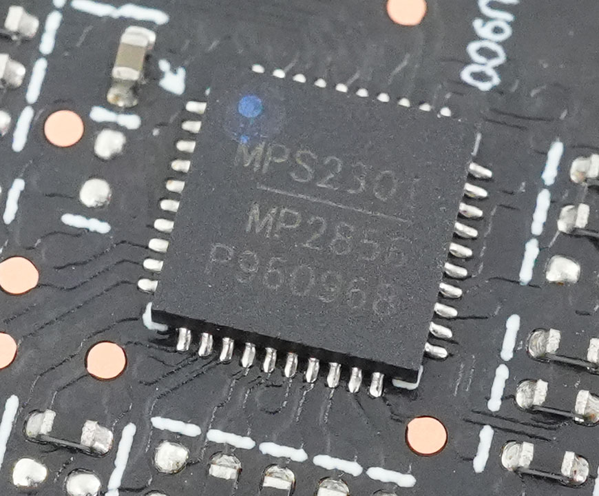

Memory voltage is a 2+1-phase design, managed by two Monolithic Power Systems MP2856 controllers.

For memory, Monolithic MP87995 DrMOS with a 70 A rating are used here, too.

The GDDR6 memory chips are made by Samsung and carry the model number K4ZAF325BC-SC20. They are specified to run at 2500 MHz (20 Gbps effective).

The GPU chip on the Radeon RX 7900 GRE is Navi 31, but it looks quite different to the chips on the RX 7900 XT and XTX. The physical size of the package is reduced, due to its roots in the mobile space. You still get the full-size GCD (graphics compute die) in the center, surrounded by four MCD (memory cache dies). The other two MCDs that you see pictured are non-functional dummies that are used to ensure structural stability of the chip, when a cooler is pushing down on it. While they look similar, the MCDs are not HBM chips. The MCDs are fabricated on a 6 nm process at TSMC Taiwan with a die size of 36.6 mm² each, the GCD is fabricated using TSMC's 5 nanometer node, with a die size of 300 mm². The combined transistor count of the GPU is 57.7 billion.
Our Patreon Silver Supporters can read articles in single-page format.
May 21st, 2024 09:11 EDT
change timezone
Latest GPU Drivers
New Forum Posts
- Ryzen 5 5600x stock overclocked reaching high temps (12)
- What's your latest tech purchase? (20607)
- My anti budget PC (60)
- What are you playing? (20722)
- MSI RX 580 Armor 8GB VBios (2)
- LG OLED C1 TV odd behaviour after nearly 2 years (57)
- Does a faster NVMe make any difference? (18)
- Would you pay more for hardware with AI capabilities? (51)
- Dell 5400 TPL Help (5)
- EK seems to be having major issues (126)
Popular Reviews
- Ghost of Tsushima Performance Benchmark Review - 35 GPUs Tested
- Ghost of Tsushima: DLSS vs. FSR vs. XeSS Comparison Review
- PNY XLR8 Gaming EPIC-X RGB DDR5-6400 CL32 32 GB Review
- TerraMaster D8 Hybrid Review
- Silverstone Shark Force 120 mm Fan Review
- Homeworld 3 Performance Benchmark Review - 35 GPUs Tested
- Upcoming Hardware Launches 2023 (Updated Feb 2024)
- Lofree Edge Ultra-Low Profile Wireless Mechanical Keyboard Review
- AMD Ryzen 7 7800X3D Review - The Best Gaming CPU
- AMD Ryzen 7 7700 Review - Affordable Zen 4 Powerhouse
Controversial News Posts
- Intel Statement on Stability Issues: "Motherboard Makers to Blame" (269)
- AMD to Redesign Ray Tracing Hardware on RDNA 4 (227)
- Windows 11 Now Officially Adware as Microsoft Embeds Ads in the Start Menu (173)
- NVIDIA to Only Launch the Flagship GeForce RTX 5090 in 2024, Rest of the Series in 2025 (154)
- AMD Hits Highest-Ever x86 CPU Market Share in Q1 2024 Across Desktop and Server (140)
- AMD RDNA 5 a "Clean Sheet" Graphics Architecture, RDNA 4 Merely Corrects a Bug Over RDNA 3 (139)
- AMD's RDNA 4 GPUs Could Stick with 18 Gbps GDDR6 Memory (114)
- AMD Ryzen 9 7900X3D Now at a Mouth-watering $329 (104)