 59
59
Zotac GeForce GTX 260 Amp² Edition 216 Shaders Review
(59 Comments) »Introduction
Today NVIDIA launches their updated GeForce GTX 260 Series. The new cards feature an increased shader count of 216 versus 192 on the "normal" GTX 260. Yet there is no new product name by NVIDIA, the product is still called GTX 260. I am not sure if this is a good move because it will create a lot of confusion with the users. Calling it GTX 270 or even GTX 260+ would have been a better strategy in my opinion. As confirmed by NVIDIA this is the same GPU as on the GTX 260 and GTX 280, just with a different number of shaders and texture units. The silicon has remained the same, which means it is still a 65 nm design - a shrinked 55 nm version will follow later this year. Also it should be noted that this 216 shader GPU will not completely replace the GTX 260 with 192 shaders. There will just be three GT200 based products in the future.
Zotac has labeled their card GTX 260 AMP² Edition, a non-AMP card will be available as well with lower clocks but still 216 shaders.
For your reference, see our previous reviews of the GTX 260 and GTX 280:
- Zotac GeForce GTX 280 Amp! Edition
- Point of View GeForce GTX 280 Assassins Creed Edition
- Point of View GeForce GTX 260 Assassins Creed Edition
| GeForce 8800 GT | GeForce 9800 GT | Radeon HD 4850 | GeForce 9800 GTX | GeForce 9800 GTX+ | GeForce 8800 GTX | GeForce GTX 260 | Radeon HD 4870 | Zotac GTX 260 Amp² | GeForce GTX 280 | Radeon HD 4870 X2 | |
| Shader units | 112 | 112 | 800 | 128 | 128 | 128 | 192 | 800 | 216 | 240 | 2x 800 |
| ROPs | 16 | 16 | 16 | 16 | 16 | 24 | 28 | 16 | 28 | 32 | 2x 16 |
| GPU | G92 | G92 | RV770 | G92 | G92 | G80 | GT200 | RV770 | GT200 | GT200 | 2x RV770 |
| Transistors | 754M | 754M | 956M | 754M | 754M | 681M | 1400M | 956M | 1400M | 1400M | 2x 956M |
| Memory Size | 512 MB | 512 MB | 512 MB | 512 MB | 512 MB | 768 MB | 896 MB | 512 MB | 896 MB | 1024 MB | 2x 1024 MB |
| Memory Bus Width | 256 bit | 256 bit | 256 bit | 256 bit | 256 bit | 384 bit | 448 bit | 256 bit | 448 bit | 512 bit | 2x 256 bit |
| Core Clock | 600 MHz | 600 MHz | 625 MHz | 675 MHz | 738 MHz | 575 MHz | 576 MHz | 750 MHz | 650 MHz | 602 MHz | 750 MHz |
| Memory Clock | 900 MHz | 900 MHz | 993 MHz | 1100 MHz | 1100 MHz | 900 MHz | 999 MHz | 900 MHz | 1050 MHz | 1107 MHz | 900 MHz |
| Price | $140 | $160 | $170 | $185 | $200 | $295 | $270 | $280 | $299 | $430 | $550 |
Packaging & Contents

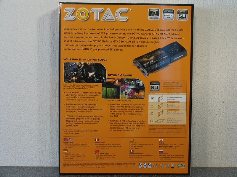
Even the package of the GTX 260 AMP² is the same, the only difference is an AMP2! sticker on the package.
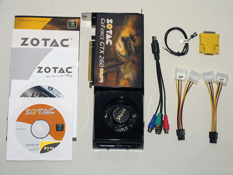
You will receive:
- Graphics card
- Manual + Warranty card + Quickstart Guide
- Driver CD
- Racedriver GRID full game
- DVI adapter, HDMI adapter
- Video out cable
- PCI-Express adapter cables
The Card
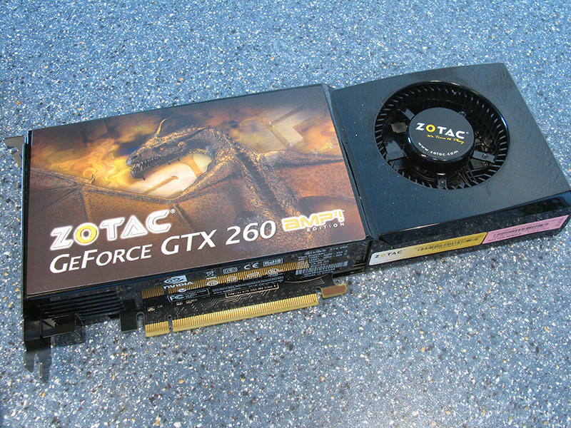

The card looks exactly the same as the GeForce GTX 260 and GTX 280, the only visible difference are the stickers on the card and on the cooler.

The card has two DVI ports which is the standard output configuration nowadays. If you need a VGA port you can use the included DVI adapter. When using a HDMI adapter (included as well), you will also have access to HDMI+HDCP+Audio, which allows easy setup of a media PC. NVIDIA's HDMI Audio design requires you to feed an audio signal to the card so it can be added to the HDMI Video stream from the card.
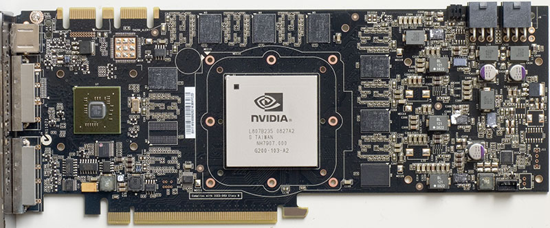

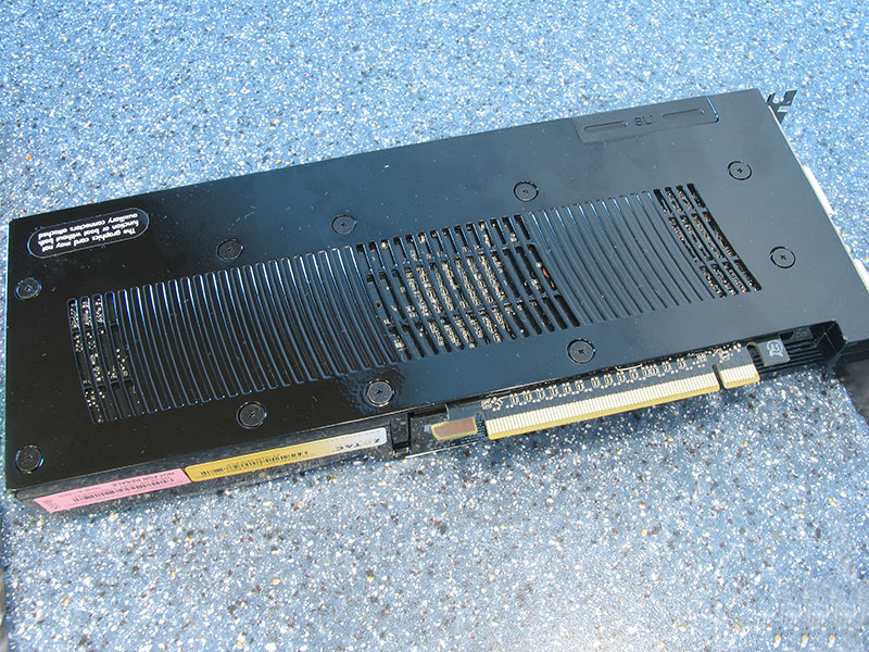
Here are the front and the back of the card, high-res versions are also available (front, back). If you choose to use these images for voltmods etc, please include a link back to this site or let us post your article.
A Closer Look


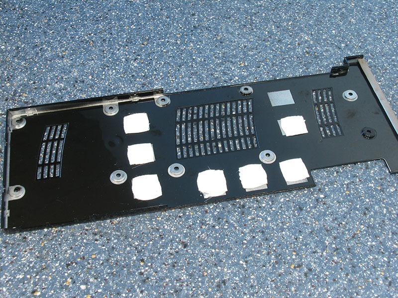
The cooler has remained the same big heatsink that is used on the GTX 260 and GTX 280. If you look closely you can see that two memory cooling spots are not populated which accounts for the memory difference from 1024 MB to 896 MB (compared to the GTX280).

You may combine two or three cards for SLI to improve framerates or graphics quality.

Just like the regular GTX 260, the GTX 260 AMP2 requires two six-pin PCI-Express power connectors.
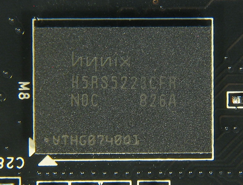
The GDDR3 memory chips are made by Hynix and carry the model number H5RS5223CFR-N0C. With a latency of 1.0 ns they should be good for at least 1000 MHz.
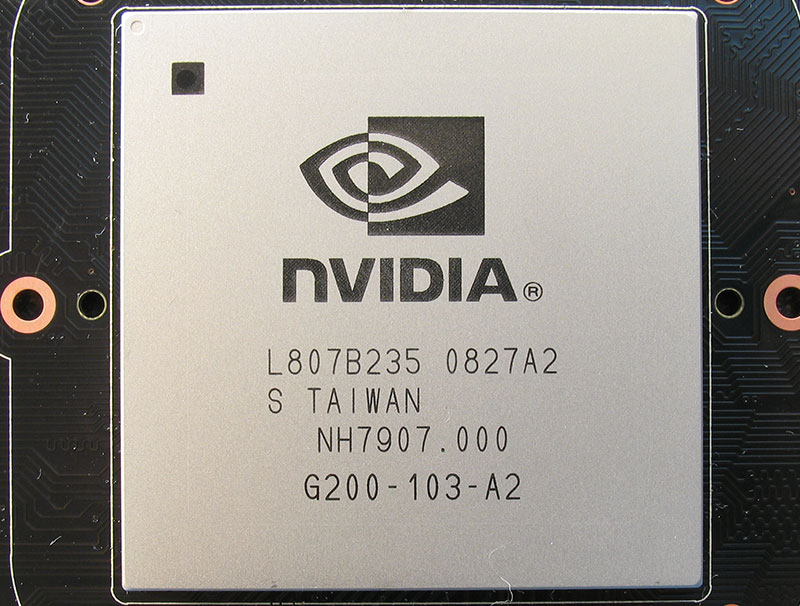
This is NVIDIA's massive GT200 GPU, it comes with 1.4 billion transistors in a 65 nm process. Its die size of 576 mm² makes it the biggest and most expensive GPU produced to date. Please note that the metal you see is not the GPU die, but the heatspreader on top of it.
Our Patreon Silver Supporters can read articles in single-page format.
May 15th, 2024 20:00 EDT
change timezone
Latest GPU Drivers
New Forum Posts
- 24-pin connector won’t snap onto motherboard (3)
- Post Your TIMESPY, PCMARK10 & FIRESTRIKE SCORES! (2019) (219)
- Ryzen Owners Zen Garden (7356)
- AM5 boot times improve RADICALLY with memory context restore enabled (68)
- Would you pay more for hardware with AI capabilities? (16)
- Laptop i7 11800H Throttling Immediately (12)
- RMAd every single component in my PC, and it's still crashing (11)
- Regular frametime spikes in all games (12)
- 20 Years? (10)
- Speed Shift settings to explain (5)
Popular Reviews
- Homeworld 3 Performance Benchmark Review - 35 GPUs Tested
- Enermax REVOLUTION D.F. X 1200 W Review
- Lofree Edge Ultra-Low Profile Wireless Mechanical Keyboard Review
- ZMF Caldera Closed Planar Magnetic Headphones Review
- Upcoming Hardware Launches 2023 (Updated Feb 2024)
- Corsair MP700 Pro SE 4 TB Review
- AMD Ryzen 7 7800X3D Review - The Best Gaming CPU
- ThundeRobot ML903 NearLink Review
- Bykski CPU-XPR-C-I CPU Water Block Review - Amazing Value!
- ASUS Radeon RX 7900 GRE TUF OC Review
Controversial News Posts
- Intel Statement on Stability Issues: "Motherboard Makers to Blame" (267)
- AMD to Redesign Ray Tracing Hardware on RDNA 4 (227)
- Windows 11 Now Officially Adware as Microsoft Embeds Ads in the Start Menu (172)
- NVIDIA to Only Launch the Flagship GeForce RTX 5090 in 2024, Rest of the Series in 2025 (152)
- AMD Hits Highest-Ever x86 CPU Market Share in Q1 2024 Across Desktop and Server (137)
- AMD RDNA 5 a "Clean Sheet" Graphics Architecture, RDNA 4 Merely Corrects a Bug Over RDNA 3 (123)
- AMD's RDNA 4 GPUs Could Stick with 18 Gbps GDDR6 Memory (114)
- AMD Ryzen 9 7900X3D Now at a Mouth-watering $329 (104)