 68
68
ASUS GeForce GTX 470 Fermi Review
The Card »Introduction

A few weeks back NVIDIA launched what is certainly the most anticipated graphics card series this year. The NVIDIA GeForce GTX 470 and 480 are based on NVIDIA's new Fermi architecture which is a complete overhaul of the GT200 architecture. The cards offer full support for DirectX 11 and Tesselation, as well as 3D Vision Surround for multi-monitor gaming in 3D.

The GeForce GTX 470 is based on the same Fermi core as the GTX 480 but uses a reduced shader count and less memory bus width. In the image above, you can see the disabled components of the GF100 GPU. Please note that the red rectangles can be any SM or any MC, not specifically the marked ones. This allows NVIDIA to harvest more GPUs from their production which results in a more economic end-user pricing of the product.
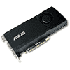
ASUS has sent us a final retail sample of GeForce GTX 470.
| Radeon HD 4870 X2 | GeForce GTX 285 | Radeon HD 5850 | GeForce GTX 470 | Radeon HD 5870 | GeForce GTX 480 | GeForce GTX 295 | Radeon HD 5970 | |
| Shader units | 2x 800 | 240 | 1440 | 448 | 1600 | 480 | 2x 240 | 2x 1600 |
| ROPs | 2x 16 | 32 | 32 | 40 | 32 | 48 | 2x 28 | 2x 32 |
| GPU | 2x RV770 | GT200b | Cypress | GF100 | Cypress | GF100 | 2x GT200b | 2x Cypress |
| Transistors | 2x 956M | 1400M | 2154M | 3200M | 2154M | 3200M | 2x 1400M | 2x 2154M |
| Memory Size | 2x 1024 MB | 1024 MB | 1024 MB | 1280 MB | 1024 MB | 1536 MB | 2x 896 MB | 2x 1024 MB |
| Memory Bus Width | 2x 256 bit | 512 bit | 256 bit | 320 bit | 256 bit | 384 bit | 2x 448 bit | 2x 256 bit |
| Core Clock | 750 MHz | 648 MHz | 725 MHz | 607 MHz | 850 MHz | 700 MHz | 576 MHz | 725 MHz |
| Memory Clock | 900 MHz | 1242 MHz | 1000 MHz | 837 MHz | 1200 MHz | 924 MHz | 999 MHz | 1000 MHz |
| Price | $350 | $350 | $310 | $349 | $400 | $499 | $520 | $630 |
Packaging & Contents
We received a retail card, but without packaging and accessories.
Apr 6th, 2025 07:42 EDT
change timezone
Latest GPU Drivers
New Forum Posts
- What are you playing? (23345)
- Dune: Awakening benchmark - post your results (51)
- RX 9000 series GPU Owners Club (184)
- DTS DCH Driver for Realtek HDA [DTS:X APO4 + DTS Interactive] (2129)
- EK Quantum Velocity intel to amd conversion (11)
- AMD RX 9070 XT & RX 9070 non-XT thread (OC, undervolt, benchmarks, ...) (78)
- 9800x3d for 1440p gaming? (26)
- Will you buy a RTX 5090? (467)
- gpu heirarchy/performance/benchmarks- whos lying? (34)
- need help choosing an upgrade (17)
Popular Reviews
- ASUS Prime X870-P Wi-Fi Review
- PowerColor Radeon RX 9070 Hellhound Review
- Corsair RM750x Shift 750 W Review
- UPERFECT UStation Delta Max Review - Two Screens In One
- DDR5 CUDIMM Explained & Benched - The New Memory Standard
- Upcoming Hardware Launches 2025 (Updated Apr 2025)
- Sapphire Radeon RX 9070 XT Pulse Review
- Sapphire Radeon RX 9070 XT Nitro+ Review - Beating NVIDIA
- AMD Ryzen 7 9800X3D Review - The Best Gaming Processor
- Pwnage Trinity CF Review
Controversial News Posts
- MSI Doesn't Plan Radeon RX 9000 Series GPUs, Skips AMD RDNA 4 Generation Entirely (146)
- Microsoft Introduces Copilot for Gaming (124)
- AMD Radeon RX 9070 XT Reportedly Outperforms RTX 5080 Through Undervolting (119)
- NVIDIA GeForce RTX 5060 Ti 16 GB SKU Likely Launching at $499, According to Supply Chain Leak (115)
- NVIDIA Reportedly Prepares GeForce RTX 5060 and RTX 5060 Ti Unveil Tomorrow (115)
- Over 200,000 Sold Radeon RX 9070 and RX 9070 XT GPUs? AMD Says No Number was Given (100)
- NVIDIA GeForce RTX 5050, RTX 5060, and RTX 5060 Ti Specifications Leak (97)
- Nintendo Switch 2 Launches June 5 at $449.99 with New Hardware and Games (92)