 25
25
HIS Radeon HD 6850 1 GB Review
Packaging & Contents »Introduction
The day we've been waiting for since the past couple of months has finally arrived. AMD, which pioneered DirectX 11 compliant PC consumer graphics, is out with its second-generation DirectX 11 architecture, codenamed Northern Islands. The company has enjoyed a 6 month head-start into the race for DirectX 11 graphics hardware market dominance, which also reflected in both growth of market-share, and domination in sales. The time passed by also allowed AMD to refine and fine-tune its architecture to better suit the existing 40 nm silicon fabrication process, by promising to churn out higher performance per Watt and performance per mm² of die-area (plays an important role in product pricing), compared to the previous-generation Evergreen architecture.
The new architecture also refines and expands on the product's feature-set, giving the GPU an even bigger role to play in today's PC than simply rendering 3D graphics: that's accelerating smooth and crystal-clear high-definition video, and getting into CPU territory, by number-crunching for applications at a much more parallel scale than multicore processors.
The product also marks a fundamental shift in AMD's approach to the market. Until now, the HD x800 series (such as HD 3800 series, HD 4800 series, and HD 5800 series) is regarded as that class of SKUs that give you the highest single-GPU performance possible for the prevalent architecture. But now, AMD has restructured its nomenclature in a big way.
When it came to light that Barts, oversimplistically a successor to the Juniper GPU (which makes up the Radeon HD 5700 series), is going to be branded under the HD 6800 series, it created quite some drama; with some users claiming it to be very gimmicky of AMD to release a series that isn't much of an upgrade option for existing users of HD 5800 series GPUs. That's not the case, because AMD made it adequately public through the press, its reasoning behind using the HD 6800 series as the "gamer's sweet spot" series, and consolidating all higher-end SKUs into the Radeon HD 6900 series, slated for next month. Besides, it's not like AMD is asking Radeon HD 5800 series kind of prices for today's GPUs. The main design ideology behind the HD 6800 series, as AMD put it, is to give you Radeon HD 5800 series performance at sweet-spot prices.
The HIS Radeon HD 6850 1 GB we're reviewing today is a remixed AMD reference design implementation by HIS that makes use of a cooler that's similar to AMD's cost-effective reference design GPU cooler. The PCB is AMD reference design, but is colored blue.

One major issue with the sample I received was that it came with 1120 shaders enabled. The HD 6850 specification requires 960 shaders. Unfortunately neither HIS, nor AMD could provide help with getting the board fixed so I had to reconfigure the shaders on my own. This review shows the correct performance numbers you should expect from a 960 shader HD 6850. If you see other HD 6850 reviews on the web that show surprisingly high performance, please ask the reviewer to check fillrate or using GPU-Z. I know of one other site who received a Sapphire HD 6850 with 1120 shaders enabled, so the problem might be more widespread.
Architecture
Barts, named after the Saint Barthélemy island in the Caribbean, is a performance-segment GPU. It is built on the 40 nm silicon fabrication process at TSMC, Taiwan. Since it is essentially a DirectX 11 generation GPU, most of the components are the same as on the Radeon HD 5000, albeit with a lot of restructuring. The SIMD processing area, like on the Cypress, is branched into two blocks, because there are way too many SIMD units. While Cypress had a single Ultra-Threaded Dispatch Processor component that semaphored instructions and data between the two clusters, with Barts, AMD gave each cluster its own dispatch processor, instruction and constant caches, thus increasing the parallelism. Each cluster holds 7 SIMD engines, with 80 stream processors, each. On the HD 6850, two of these SIMD engines are disabled, leaving us 960 stream processors. Coupled with engine clock speeds of 775 MHz, the computational power of Barts in its Radeon HD 6850 avatar, hence, is rated at 1.5 TFLOPS.There are 48 texture units (TMUs) available on Radeon HD 6850. With a 256-bit wide GDDR5 memory interface, there are 32 raster operations processors (ROPs). AMD also addressed the one shortcoming of the Evergreen architecture which NVIDIA took advantage of: tessellation performance. Northern Islands GPUs carry a second generation tessellation unit that is both redesigned, and is backed by a new adaptive tessellation algorithm at the driver level. Together, up to 100% increase in tessellation performance is advertised by AMD.
A more detailed Architecture overview is available in our HD 6870 review.
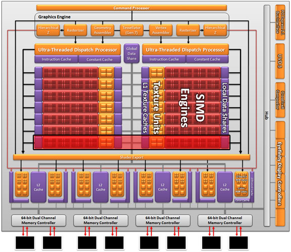
There is a redesigned video acceleration component, the 3rd generation Unified Video Decoder (UVD 3.0), which provides GPU acceleration for Blu-ray 3D and DivX high-definition video formats, and six display controllers offering six TMDS links. This lets users connect up to six displays to as independent display heads, or span display heads across multiple physical displays using the Eyefinity technology. The new HDMI 1.4a connector standard is made use of, which gives you support for stereoscopic 3D standards such as Blu-ray 3D, the two mini-DisplayPort 1.2 connectors support Multi-Stream technology that let you daisy-chain 3 physical displays per connector, letting you wrap up a 6-display Eyefinity array using just those two connectors.
| Radeon HD 5770 | GeForce GTX 460 | GeForce GTX 460 | Radeon HD 6850 | Radeon HD 5850 | GeForce GTX 470 | Radeon HD 6870 | Radeon HD 5870 | GeForce GTX 480 | Radeon HD 5970 | |
| Shader units | 800 | 336 | 336 | 960 | 1440 | 448 | 1120 | 1600 | 480 | 2x 1600 |
| ROPs | 16 | 24 | 32 | 32 | 32 | 40 | 32 | 32 | 48 | 2x 32 |
| GPU | Juniper | GF104 | GF104 | Barts | Cypress | GF100 | Barts | Cypress | GF100 | 2x Cypress |
| Transistors | 1040M | 1950M | 1950M | 1700M | 2154M | 3200M | 1700M | 2154M | 3200M | 2x 2154M |
| Memory Size | 1024 MB | 768 MB | 1024 MB | 1024 MB | 1024 MB | 1280 MB | 1024 MB | 1024 MB | 1536 MB | 2x 1024 MB |
| Memory Bus Width | 128 bit | 192 bit | 256 bit | 256 bit | 256 bit | 320 bit | 256 bit | 256 bit | 384 bit | 2x 256 bit |
| Core Clock | 850 MHz | 675 MHz | 675 MHz | 775 MHz | 725 MHz | 607 MHz | 900 MHz | 850 MHz | 700 MHz | 725 MHz |
| Memory Clock | 1200 MHz | 900 MHz | 900 MHz | 1000 MHz | 1000 MHz | 837 MHz | 1050 MHz | 1200 MHz | 924 MHz | 1000 MHz |
| Price | $140 | $160 | $200 | $180 | $260 | $260 | $240 | $360 | $450 | $580 |
Apr 24th, 2024 17:59 EDT
change timezone
Latest GPU Drivers
New Forum Posts
- Is there a technical reason that Windows 11 doesn't have built into it battery charge limitation? (41)
- Best SSD for system drive (75)
- How are MX330 and İ5 1135G7 ? (9)
- GTX 1070 Ti - TDP Issues - Always Power Throttling (1)
- Will a RTX 4070 TI super bottleneck a Ryzen 9 7950X3D? (55)
- 3DMARK "LEGENDARY" (189)
- TPU's Nostalgic Hardware Club (18462)
- Meta Horizon OS (14)
- im new to throttelstop and i think i messed it up by copying others any hints would be very much aprreciated (0)
- Is It The 1080 TI The Best GPU Ever? (214)
Popular Reviews
- Fractal Design Terra Review
- Thermalright Phantom Spirit 120 EVO Review
- Corsair 2000D Airflow Review
- Minisforum EliteMini UM780 XTX (AMD Ryzen 7 7840HS) Review
- ASUS GeForce RTX 4090 STRIX OC Review
- NVIDIA GeForce RTX 4090 Founders Edition Review - Impressive Performance
- ASUS GeForce RTX 4090 Matrix Platinum Review - The RTX 4090 Ti
- MSI GeForce RTX 4090 Gaming X Trio Review
- MSI GeForce RTX 4090 Suprim X Review
- Gigabyte GeForce RTX 4090 Gaming OC Review
Controversial News Posts
- Sony PlayStation 5 Pro Specifications Confirmed, Console Arrives Before Holidays (116)
- NVIDIA Points Intel Raptor Lake CPU Users to Get Help from Intel Amid System Instability Issues (106)
- AMD "Strix Halo" Zen 5 Mobile Processor Pictured: Chiplet-based, Uses 256-bit LPDDR5X (101)
- US Government Wants Nuclear Plants to Offload AI Data Center Expansion (98)
- Windows 10 Security Updates to Cost $61 After 2025, $427 by 2028 (84)
- Developers of Outpost Infinity Siege Recommend Underclocking i9-13900K and i9-14900K for Stability on Machines with RTX 4090 (84)
- TechPowerUp Hiring: Reviewers Wanted for Motherboards, Laptops, Gaming Handhelds and Prebuilt Desktops (78)
- Intel Realizes the Only Way to Save x86 is to Democratize it, Reopens x86 IP Licensing (70)