 24
24
HIS Radeon HD 6950 2 GB Review
Test Setup »A Closer Look
The first piece to come off the card is the backplate. It serves no special purpose other than to protect the card from physical damage and spread the heat around a bit. Since there are no memory chips or other important circuitry on this side of the card, there is no need for a backplate to cool them.
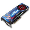
The AMD reference cooler uses a big vapor chamber base to transfer heat away quickly from the GPU. In addition to the GPU, you can also see cooling pads for memory and voltage regulation circuitry.
The Radeon HD 6950 uses a 6+6 power input configuration.
AMD has added a small switch near the card that lets you toggle between two VGA BIOSes. The first one is the normal one and can be flashed. The second one acts as backup and is write-protected, so you can not "destroy" it in case of a bad flash. Should you flash your card with the wrong BIOS, you can switch to the backup BIOS to boot the card, then change the switch to the normal BIOS before flashing. This looks like a good system, but I wonder if it's worth the added cost.
The GDDR5 memory chips are made by Hynix, and carry the model number H5GQ2H24MFR-T2C. They are specified to run at 1250 MHz (5000 MHz GDDR5 effective).
The Radeon HD 6900 Series are the first graphics cards to use the Volterra VT1556. It offers extensive voltage control and monitoring via I2C. At this time no software supports this controller yet, but I am sure this will change in the weeks to come.
AMD's new Cayman graphics processor is made on a 40 nm process at TSMC Taiwan. It uses approximately 2.64 billion transistors on a die area of 389 mm².
Mar 15th, 2025 17:51 EDT
change timezone
Latest GPU Drivers
New Forum Posts
- First Build Won't Boot - Yellow DRAM Light on ASUS Prime B550M-A WiFi II (1)
- Are game requirements and VRAM usage a joke today? (608)
- I can't find my chipset drivers in device manager, do I just not have them installed? I'm on an Intel CPU. (6)
- Recommended PhysX card for 5xxx series? [Is vRAM relevant?] (166)
- Defective rtx 3080ti, Help! (1)
- HP say: Oops, we did it again ! (7)
- UPS questions (33)
- And so... I bought Arrow Lake (13700k to 265k), my thoughts. (60)
- Nvidia's GPU market share hits 90% in Q4 2024 (gets closer to full monopoly) (1003)
- DMM with PTC fuse (2)
Popular Reviews
- AMD Ryzen 9 9950X3D Review - Great for Gaming and Productivity
- Sapphire Radeon RX 9070 XT Nitro+ Review - Beating NVIDIA
- Gigabyte X870E Aorus Pro Review
- FSP MP7 Black Review
- XFX Radeon RX 9070 XT Mercury OC Magnetic Air Review
- ASUS GeForce RTX 5090 TUF Review
- MSI GeForce RTX 5070 Gaming Trio OC Review
- ASUS Radeon RX 9070 TUF OC Review
- VAXEE Zygen NP-01S V2 Wireless Review
- Dough Spectrum Black 32 Review
Controversial News Posts
- NVIDIA GeForce RTX 50 Cards Spotted with Missing ROPs, NVIDIA Confirms the Issue, Multiple Vendors Affected (513)
- AMD RDNA 4 and Radeon RX 9070 Series Unveiled: $549 & $599 (260)
- AMD Mentions Sub-$700 Pricing for Radeon RX 9070 GPU Series, Looks Like NV Minus $50 Again (249)
- NVIDIA Investigates GeForce RTX 50 Series "Blackwell" Black Screen and BSOD Issues (244)
- AMD Radeon RX 9070 and 9070 XT Official Performance Metrics Leaked, +42% 4K Performance Over Radeon RX 7900 GRE (195)
- AMD Radeon RX 9070-series Pricing Leaks Courtesy of MicroCenter (158)
- AMD Radeon RX 9070 XT Reportedly Outperforms RTX 5080 Through Undervolting (116)
- Microsoft Introduces Copilot for Gaming (107)


