 94
94
ZOTAC GeForce GTX 465 Review
Packaging & Contents »Introduction

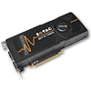
Today NVIDIA launches their GeForce GTX 465 Series. Like all other GTX 400 cards so far, the GTX 465 is based on NVIDIA GF100 "Fermi" GPU. NVIDIA positions their latest child in the sub-$300 market with an MSRP of $279. ZOTAC has sent us their GeForce GTX 465 which is the same as any other GTX 465 reference design, with the only difference being the sticker on the cooler and the bundle.

In order to meet their price/performance target, NVIDIA has disabled large sections of the GF100 GPU. This approach also gives NVIDIA the opportunity to sell GPUs that didn't qualify to be used on higher-end cards like the GeForce GTX 470 or 480. On the picture above, I have marked disabled sections in red. Please note that the "location" of the red boxes can be changed by NVIDIA to optimize their GPU harvesting - it's the number of enabled units that matters for the product to be called GTX 465.
| Radeon HD 5830 | GeForce GTX 275 | GeForce GTX 465 | GeForce GTX 285 | Radeon HD 5850 | GeForce GTX 470 | Radeon HD 5870 | GeForce GTX 480 | |
| Shader units | 1120 | 240 | 352 | 240 | 1440 | 448 | 1600 | 480 |
| ROPs | 16 | 28 | 32 | 32 | 32 | 40 | 32 | 48 |
| GPU | Cypress | GT200 | GF100 | GT200 | Cypress | GF100 | Cypress | GF100 |
| Transistors | 2154M | 1404M | 3200M | 1404M | 2154M | 3200M | 2154M | 3200M |
| Memory Size | 1024 MB | 896 MB | 1024 MB | 1024 MB | 1024 MB | 1280 MB | 1024 MB | 1536 MB |
| Memory Bus Width | 256 bit | 448 bit | 256 bit | 512 bit | 256 bit | 320 bit | 256 bit | 384 bit |
| Core Clock | 800 MHz | 602 MHz | 607 MHz | 648 MHz | 725 MHz | 607 MHz | 850 MHz | 700 MHz |
| Memory Clock | 1000 MHz | 1107 MHz | 802 MHz | 1242 MHz | 1000 MHz | 837 MHz | 1200 MHz | 924 MHz |
| Price | $230 | $230 | $279 | $350 | $310 | $349 | $400 | $499 |
Apr 8th, 2025 05:30 EDT
change timezone
Latest GPU Drivers
New Forum Posts
- Asus X670E Crosshair Crashes (8)
- is it worth using ssd with usb2? (13)
- Is RX 9070 VRAM temperature regular value or hotspot? (330)
- RX 9000 series GPU Owners Club (238)
- 5070 cards available below £550 in in the UK (76)
- 9070XT or 7900XT or 7900XTX (130)
- The easiest way to connect the BOOTSEL test metal terminal and the GND terminal.... (2)
- gpu heirarchy/performance/benchmarks- whos lying? (67)
- Sapphire NITRO+ RX 5700 XT BE original BIOS request (11)
- No idea how many watts this USB-C port will supply? (10)
Popular Reviews
- The Last Of Us Part 2 Performance Benchmark Review - 30 GPUs Compared
- UPERFECT UStation Delta Max Review - Two Screens In One
- PowerColor Radeon RX 9070 Hellhound Review
- ASUS Prime X870-P Wi-Fi Review
- Upcoming Hardware Launches 2025 (Updated Apr 2025)
- MCHOSE L7 Pro Review
- Sapphire Radeon RX 9070 XT Pulse Review
- Corsair RM750x Shift 750 W Review
- Sapphire Radeon RX 9070 XT Nitro+ Review - Beating NVIDIA
- DDR5 CUDIMM Explained & Benched - The New Memory Standard
Controversial News Posts
- NVIDIA GeForce RTX 5060 Ti 16 GB SKU Likely Launching at $499, According to Supply Chain Leak (161)
- MSI Doesn't Plan Radeon RX 9000 Series GPUs, Skips AMD RDNA 4 Generation Entirely (146)
- Microsoft Introduces Copilot for Gaming (124)
- AMD Radeon RX 9070 XT Reportedly Outperforms RTX 5080 Through Undervolting (119)
- NVIDIA Reportedly Prepares GeForce RTX 5060 and RTX 5060 Ti Unveil Tomorrow (115)
- Over 200,000 Sold Radeon RX 9070 and RX 9070 XT GPUs? AMD Says No Number was Given (100)
- NVIDIA GeForce RTX 5050, RTX 5060, and RTX 5060 Ti Specifications Leak (97)
- Nintendo Switch 2 Launches June 5 at $449.99 with New Hardware and Games (92)