Wednesday, September 13th 2023

Nintendo Switch 2 to Feature NVIDIA Ampere GPU with DLSS
The rumors of Nintendo's next-generation Switch handheld gaming console have been piling up ever since the competition in the handheld console market got more intense. Since the release of the original Switch, Valve has released Steam Deck, ASUS made ROG Ally, and others are also exploring the market. However, the next-generation Nintendo Switch 2 is closer and closer, as we have information about the chipset that will power this device. Thanks to Kepler_L2 on Twitter/X, we have the codenames of the upcoming processors. The first generation Switch came with NVIDIA's Tegra X1 SoC built on a 20 nm node. However, later on, NVIDIA supplied Nintendo with a Tegra X1+ SoC made on a 16 nm node. There were no performance increases recorded, just improved power efficiency. Both of them used four Cortex-A57 and four Cortex-A53 cores with GM20B Maxwell GPUs.
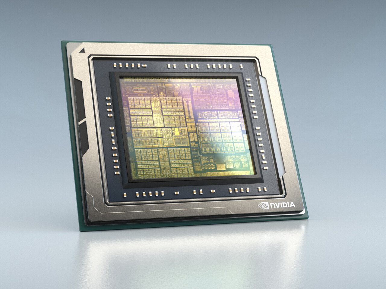
For the Nintendo Switch 2, NVIDIA is said to utilize a customized variant of NVIDIA Jetson Orin SoC for automotive applications. The reference Orin SoC carries a codename T234, while this alleged adaptation has a T239 codename; the version is most likely optimized for power efficiency. The reference Orin design is a considerable uplift compared to the Tegra X1, as it boasts 12 Cortex-A78AE cores and LPDDR5 memory, along with Ampere GPU microarchitecture. Built on Samsung's 8 nm node, the efficiency would likely yield better battery life and position the second-generation Switch well among the now extended handheld gaming console market. However, including Ampere architecture would also bring technologies like DLSS, which would benefit the low-power SoC.
Sources:
@Kepler_L2, GitHub, via Tom's Hardware
For the Nintendo Switch 2, NVIDIA is said to utilize a customized variant of NVIDIA Jetson Orin SoC for automotive applications. The reference Orin SoC carries a codename T234, while this alleged adaptation has a T239 codename; the version is most likely optimized for power efficiency. The reference Orin design is a considerable uplift compared to the Tegra X1, as it boasts 12 Cortex-A78AE cores and LPDDR5 memory, along with Ampere GPU microarchitecture. Built on Samsung's 8 nm node, the efficiency would likely yield better battery life and position the second-generation Switch well among the now extended handheld gaming console market. However, including Ampere architecture would also bring technologies like DLSS, which would benefit the low-power SoC.
117 Comments on Nintendo Switch 2 to Feature NVIDIA Ampere GPU with DLSS
The VRAM alone on that GPU would use more power than the entire devices power budget
Yeah that gddr6 is probably taking the majority of that 30 watts.
Good thing there's lpddr.
My real point was this:The NVidia SOC Nintendo is reported to be using is very capible and while some visual effect will have to be scaled down, playable 4k30 or 4k60 is not outside the realm of possibility. For anyone to make the blanket statement that it's NOT possible needs to take a step back and look at the bigger picture for the simple reason that the Jetson Platform can already do so and the Nintendo SOC is going to be a customized and enhanced version of that.
We know the architecture, the number of cuda cores, the tensor cores, the tmu's the rops.
We know the bus width, we know the ram type. We know it's a unified memory architecture.
We have literally never known this much about a nintendo system so early ever.
There is literally precious little mystery for your appeal to the mysterious.
Things are just getting absurd and derailed in here.
*Edit* Somebody reminded me that I forgot ultra performance is no longer 8k only, so all you need for ultra performance 4k is 720p, and 360p for ultr perf to 1080 for portable.*
We know the clock speeds and the render config from the stolen nvn2 api. The wattage is a function of the lithography and feature set.
1536 ampere cuda cores downclocked to 1ghz (the nvn2 test docked clock was something like 1.125 GHz btw, ive been low balling) is 3.072 tflops for fp32, and 24.576 tflops sparse fp16 on the tensor cores for dlss.
It has a dual channel 128 bit bus for its lpddr5, for a standard 102 gbps.
It will be able to handle 1080p 60 native just fine if someone wants to target that, and the stated performance must be within the target tdp, or it would have never been taped out. And again, 1080p is all you need for a 4k input res.
One of the closed doors demos nintendo showed off at gamescom was botw, literally running at 4k60 fps with no loading times.
Nintendo probably wouldn't be showing this to people they want to make games for their system, if it wasn't something that was feasible to do.... or that they did not have the intent of doing themselves.
4k 120 is ridiculous, 4k 60 docked is going to happen on the system, just like 1080p 60fps happened on switch. Like switch It's not going to be the standard, and its mostly going to be switch and ps4/xbone ports, but it's going to happen.Scene Complexity doesn't really directly matter for dlss, it's a fixed render time based on input resolution to output resolution, no matter how simple or complex the fidelity of the source inputs are.
Using quality or balanced mode, is likely something that will never happen on this system, it will almost undoubtedly always be performance.
If they were targeting 1440p, the input res would be 720p. As I stated earlier, this is my bet for the standard on the system.
If you have the render time to make a 1080p frame of your desired fidelity and frequency on the cuda cores, you can run dlss performance to 4k on the tensor cores. Concurrently. I really can't imagine anyone hitting 1080p native, and wanting to do 1440p quality instead of 4k performance on this thing.
So let's break it down:
2048 Cuda cores, 25% more to power that the 1536 in the t239
4 GB gddr6, massive power hog compared to lpddr5 in t239.
Clock 1.245 GHz, 20% faster than my downclock estimate of 1 GHz for the t239.
There are other factors I am not accounting for as I have not found isolated/normalized power draws for them, like the aux power draw shown in the power breakdown article, i dont know how that applies to the lenovo laptop, so im leaving whatever watts they may be in, same for pcb loss, and the fact the 2050 has to power 2 GPC's and the IO crossbar between them, is more additional watt expenditure over the t239, but that won't be included. So whatever we end up with, is going to be higher than if I had all the data broken down.
So let's get rid of the ram first:
Starting point, 30 watts:
Gddr6x was measured to have a power draw of 2.5 watts per GB here:
www.igorslab.de/en/350-watts-for-nvidias-new-top-of-the-line-geforce-rtx-3090-ampere-model-explained-chip-area-calculated-and-boards-compared/
However, the 2050 mobile does not appear to use gddr6x, but gddr6, gddr6x was shown by micron to have a 15% power efficiency over gddr6 here:
www.tomshardware.com/news/micron-reveals-gddr6x-details-the-future-of-memory-or-a-proprietary-dram
So 15% more than 2.5 is 2.875, 2.875 X 4Gb =11.5 watts drawn for the 4 Gb gddr6 ram.
Lpddr4, which was used in the switch, has been measured to have a power draw around 2 watts for a complete 2x 32 bit bus x3 gb capacity =6Gb unit for the familiar 25 GB/s bandwidth (switch had 2 32 bit x2 gb units for the same bus and bandwidth.) From the university of maryland Here:
www.google.com/url?sa=t&source=web&rct=j&opi=89978449&url=https://user.eng.umd.edu/~blj/papers/isca99.pdf&ved=2ahUKEwjmi7LApICCAxWtE1kFHeapDJoQFnoECA4QAQ&usg=AOvVaw19OhDE7wDcNfAAVybZSm-d
Lpddr5 has been stated by samsung to be 30% more efficient than lpddr4x shown here:
www.google.com/amp/s/www.smartprix.com/bytes/lpddr5-ram-phones/%3famp
which was stated to be 20% more power efficient over lpddr4 here:
www.google.com/amp/s/www.faceofit.com/lpddr4-vs-lpddr4x/amp/
So 70% of 2 watts = 1.4 watts, and 80% of that = 1.12 watts for a 2 unit lpddr5 block.
Gddr6 11.5 watts, - lpddr5 1.12 watts = 10.38 watts dropped just by switching to low power ram from gddr.
Now we are at 30 watts -10.38 watts, 19.62 watts.
Now let's get rid of the fan difference. The lenovo rtx 2050 being used in this example uses a 5 watt fan, sourced by searching replacement parts for it.
The switch uses a 3 watt fan, which shouldnt really need to change.
so 2 more watts down for 17.62 watts
Now we're down to the gpc/sm's cause I'm just leaving the watts from stuff I couldn't find for certain in.
So the 2050 mobile has 2058 ampere cuda cores, or 16 sm's, 25% more to power than t239.
17.62 × .75 = 13.215 watts.
And peak performance/power draw is calculated using its boost clock of 1.245, which is 20% more than 1 ghz so.
13.215 * .80 = 10.572 watts.
And that's of course, assuming T239 is still on samsung 8nm, which doesn't have to be the case.
Hmm. Isn't this interesting...
Also It's not a coincidence rich used the exact performance specs I've been listing.
On the bright side, the one part of this experiment that was really off that rich admitted he could not mitigate was the severe vram bottleneck, which was starving the tensor cores in a way that won't happen on a device with 12 GB of Unified memory. So it won't be anywhere near 18 ms. But it still will be way out of the ballpark needed for your claims.
What is shown here is that DLSS has a very high cost with such a low power GPU. Reconstructing from 720p to 4K has a cost of over 18 ms in Death Stranding, and it lowers performance by about 50% compared to native 720p.
But the chip might feature a dedicated deep learning accelerator along tensor cores, which could help significantly reduce DLSS processing time.
It's all speculation, though. But even if 4K isn't viable, 720p performance (or 1080p with DLSS) looks really good. Even Cyberpunk is playable, and that's just a PC laptop, without any dedicated console optimization.
For me personally, what will make or break this console is backwards compatibility, for both physical and digital games.
1. Orins/a100's double tensor cores/DLA is off the table.
A. You can already tell from the nvidia employees t239 initialization kernels vs the t234's it's been removed. This space is used for rt cores on rtx arches.
B. The... er... "Source" Richard was conversing with on this topic immediately confirmed it was a miscommunication after the video went live.
2. This was not because of the tensor cores, Tensor cores are massive overkill and are not the bottleneck. See the performance of the 2080ti in the dlss 3.5 programming guide. It only has 68 gen 1 tensor cores = 68/4 = equivalent of 17 gen 2 tensor cores, yet it beats the 3060ti and 3070 in dlss 4k execution time.
The bottlenecknwas the 4 GB of Vram capacity, (not bandwidth for once). This is actually demonstrated by rich in this video, in particular when he went in depth with death stranding, where the vram.was causing stuttering because it was constantly swapping in and out assets it couldn't hold.
Dlss to 4k requires 200 MB vram set aside to feed tensor core opmem for full performance, if it doesn't get it, your tensor cores stall. As clearly demonstrated, there was no way these tensor cores were getting that.