News Posts matching #Samsung

Return to Keyword Browsing

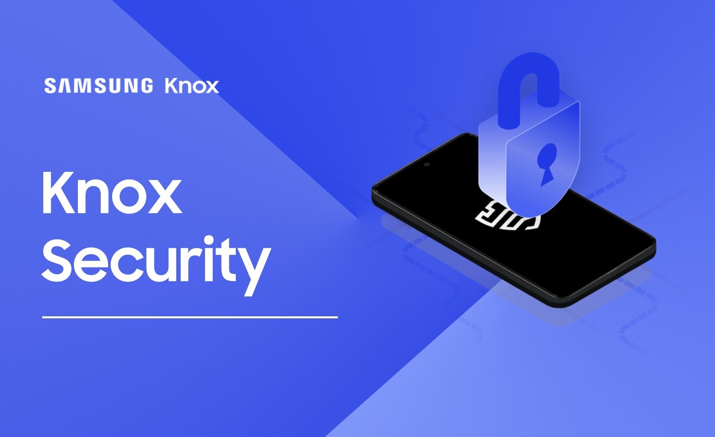
Samsung & Microsoft Reveal First On-Device Attestation Solution for Enterprise

Samsung Electronics today announced the first step in a plan to reimagine mobile device security for business customers in partnership with Microsoft. This collaboration has led to the industry's first on-device, mobile hardware-backed device attestation solution that works equally well on both company and personally owned devices.

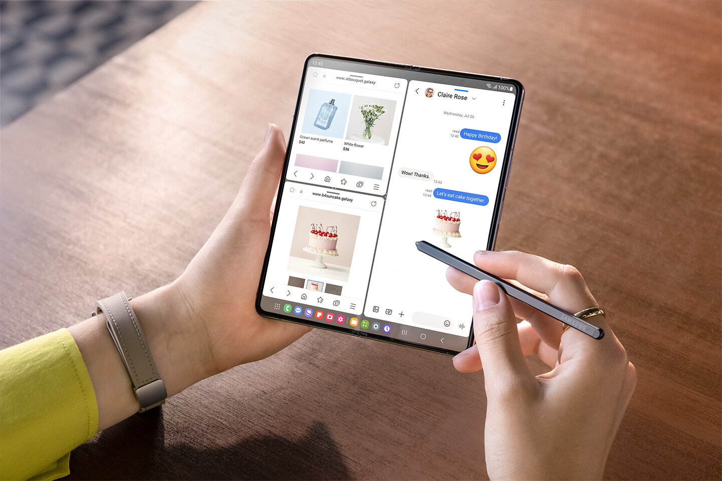
Device attestation can help ensure a device's identity and health, verifying that it has not been compromised. On-device, mobile hardware-backed device attestation—available on Samsung Galaxy devices and combined with protection from Microsoft Intune—now adds enhanced security and flexibility. For enterprises, this is an extra layer of protection against compromised devices falsely claiming to be known and healthy, gaining access to sensitive corporate data. Additionally, organizations can now enable employees to bring their own device (BYOD) to work with the confidence that they are protected with the same level of security as company owned devices. For employees, this means added flexibility for their personal Galaxy devices to safely access their work environment.

Samsung Electronics Announces Second Quarter 2023 Results

Samsung Electronics today reported financial results for the second quarter ended June 30, 2023. The Company posted KRW 60.01 trillion in consolidated revenue, a 6% decline from the previous quarter, mainly due to a decline in smartphone shipments despite a slight recovery in revenue of the DS (Device Solutions) Division. Operating profit rose sequentially to KRW 0.67 trillion as the DS Division posted a narrower loss, while Samsung Display Corporation (SDC) and the Digital Appliances Business saw improved profitability.

The Memory Business saw results improve from the previous quarter as its focus on High Bandwidth Memory (HBM) and DDR5 products in anticipation of robust demand for AI applications led to higher-than-guided DRAM shipments. System semiconductors posted a decline in profit due to lower utilization rates on weak demand from major applications.

Qualcomm Snapdragon 8 Gen 2 for Galaxy Powers Samsung's Newest Flagship Device Lineup

Qualcomm Technologies, Inc. announced that its flagship Snapdragon 8 Gen 2 Mobile Platform for Galaxy is powering Samsung Electronics Co., Ltd.'s new cutting-edge foldable smartphones, the Samsung Galaxy Z Fold5 and Galaxy Z Flip5, and its latest Galaxy Tab S9 Series. Snapdragon 8 Gen 2 for Galaxy defines a new standard for connected computing, including groundbreaking AI experiences, desktop-level gaming features, professional grade photography, and more, for consumers around the world.

"Samsung is important to our mission to deliver the world's best mobile experiences to consumers. They continue to set the pace for innovation and we couldn't be more thrilled to have Snapdragon 8 Gen 2 for Galaxy power the newest flagship Galaxy device lineup—the Galaxy Z Flip5, Galaxy Z Fold5, and Galaxy Tab S9 series," said Alex Katouzian, senior vice president and general manager, mobile, compute, & XR businesses, Qualcomm Technologies, Inc.

Samsung Also Launches the Galaxy Tab S9

Samsung Electronics Co., Ltd. announces its new Galaxy Tab S9 series, a premium product portfolio that redefines the tablet landscape and sets new standards for immersive viewing and creative freedom. Across all three models, Galaxy Tab S9, S9+ and S9 Ultra, Dynamic AMOLED 2X displays ensure epic viewing and entertainment experiences with the power of Qualcomm Snapdragon 8 Gen 2 for Galaxy. An in-box, IP68-rated S Pen helps users bring their ideas to life. And as the first Galaxy Tab S series to earn an IP68 rating, Galaxy Tab S9 series enables users to follow their inspiration, both indoors and out.

"There are no devices like the Galaxy Tab S9 series on the market today. A true disrupter in its category, it is the first of its kind to deliver experiences that users love most about tablets in one complete premium design," said TM Roh, President and Head of Mobile eXperience Business at Samsung Electronics. "The Galaxy Tab S9 series empowers users to take their big ideas and bring them to life, completely effortlessly."

Samsung Launches the Galaxy Z Flip5 and Galaxy Z Fold5

Samsung Electronics Co., Ltd. today announced its fifth generation of Galaxy foldables: Galaxy Z Flip5 and Galaxy Z Fold5. The industry-leading form factors offer unique experiences for every user with sleek and compact designs, countless customization options, and powerful performance. The new Flex Hinge makes the foldable experience possible, while offering an aesthetically balanced and solid design. These unrivalled foldable devices unlock extraordinary camera capabilities such as FlexCam to take photos from creative angles. With strong performance and an optimized battery powered by the latest processor, the Samsung Galaxy Z series transforms what is possible with a smartphone - open or closed.

"Samsung is revolutionizing the mobile industry with foldables by setting the standard and continually refining the experience," said TM Roh, President and Head of Mobile eXperience Business at Samsung Electronics. "Every day, more people choose our foldables because they offer an experience people want that they can't get on any other device. Galaxy Z Flip5 and Galaxy Z Fold5 are the latest devices that prove our commitment to meeting the needs of our customers through innovative technology."

NVIDIA is Looking at Samsung for HBM3 Memory and 2.5D Chip Packaging

According to news out of Korea, NVIDIA is considering Samsung as a partner not only for HBM3 memory, but also as a potential partner when it comes to 2.5D chip packaging. The latter is due to TSMC having limited capacity when it comes to handling all of its customers advanced chip packaging needs, although Samsung is apparently not the only potential partner NVIDIA is looking at. Taiwan based SPIL and US based Amkor Technology are two alternative candidates for the 2.5D chip packaging according to the Elec.

As far as HBM3 memory goes, NVIDIA doesn't have as many potential options, with SK Hynix being its current partner, who NVIDIA will continue to work with when it comes to HBM memory for its high-end AI accelerators and GPUs. It's likely that Samsung is trying to win NVIDIA back as a foundry customer, by proving that it's capable of handling the chip packaging for NVIDIA. Samsung will likely use its I-Cube 2.5D packaging technology and the Elec suggests that Samsung would still be using TSMC made GPU wafers which will be mated with Samsung HMB3 memory. Samsung has as yet not started its mass production of HMB3 memory, but have sampled customers with evaluation samples that are said to have received very positive feedback. For now, nothing has been agreed and TSMC is, as we know, looking to expand its 2.5D packaging business by over 40 percent, but the question is how quickly TSMC can move before its customers consider other competitors.

Samsung GDDR7 Memory Operates at Lower Voltage, Built on Same Node as 24 Gbps G6

Samsung on Wednesday announced mass-production of the world's first next-generation GDDR7 memory chips, and Ryan Smith from AnandTech scored a few technical details from the company. Apparently, the company's first production version of GDDR7 memory is built on the same D1z silicon foundry node as its 24 Gbps GDDR6 memory chip—the fastest GDDR6 chip in production. D1z is a 10 nm class foundry node that utilizes EUV lithography.

Smith also scored some electrical specs. The first-gen GDDR7 memory chip offers a data-rate of 32 Gbps at a DRAM voltage of 1.2 V, compared to the 1.35 V that some of the higher speed GDDR6 chips operate at. While the pJpb (pico-Joules per bit) is 7% higher than the current generation in absolute terms, for the 32 Gbps data-rate on offer, it is 20% lower compared to that of the 24 Gbps GDDR6 chip. Put simply, GDDR7 is 20% more energy efficient. Smith remarks that this energy-efficiency gain is purely architectural, and isn't a from any refinements to the D1z node. GDDR7 uses PAM3 signaling compared to the NRZ signaling of conventional GDDR6, and the PAM4 signalling of the GDDR6X non-JEDEC standard that NVIDIA co-developed with Micron Technology.

Samsung's 3 nm GAA Process Identified in a Crypto-mining ASIC Designed by China Startup MicroBT

Semiconductor industry research firm TechInsights said it has found that Samsung's 3 nm GAA (gate-all-around) process has been incorporated into the crypto miner ASIC (Whatsminer M56S++) from a Chinese manufacturer, MicroBT. In a Disruptive Technology Event Brief exclusively provided to DIGITIMES Asia, TechInsights points out that the significance of this development lies in the commercial utilization of GAA technology, which facilitates the scaling of transistors to 2 nm and beyond. "This development is crucial because it has the potential to enhance performance, improve energy efficiency, keep up with Moore's Law, and enable advanced applications," said TechInsights, identifying the MicroBT ASIC chip the first commercialized product using GAA technology in the industry.

But this would also reveal that Samsung is the foundry for MicroBT, using the 3 nm GAA process. DIGITIMES Research semiconductor analyst Eric Chen pointed out that Samsung indeed has started producing chips using the 3 nm GAA process, but the capacity is still small. "Getting revenues from shipment can be defined as 'commercialization', but ASIC is a relatively simple kind of chip to produce, in terms of architecture."

Samsung Announces Industry's First GDDR7 Memory Development, 32 Gbps Speeds

Samsung Electronics, a world leader in advanced semiconductor technology, today announced that it has completed development of the industry's first Graphics Double Data Rate 7 (GDDR7) DRAM. It will first be installed in next-generation systems of key customers for verification this year, driving future growth of the graphics market and further consolidating Samsung's technological leadership in the field.

Following Samsung's development of the industry's first 24 Gbps GDDR6 DRAM in 2022, the company's 16-gigabit (Gb) GDDR7 offering will deliver the industry's highest speed yet. Innovations in integrated circuit (IC) design and packaging provide added stability despite high-speed operations. "Our GDDR7 DRAM will help elevate user experiences in areas that require outstanding graphics performance, such as workstations, PCs and game consoles, and is expected to expand into future applications such as AI, high-performance computing (HPC) and automotive vehicles," said Yongcheol Bae, Executive Vice President of Memory Product Planning Team at Samsung Electronics. "The next-generation graphics DRAM will be brought to market in line with industry demand and we plan on continuing our leadership in the space."

DEEPX Announces State-of-the-Art AI Chip Product Lineup

DEEPX, a leading AI semiconductor technology company, aims to drive innovation in the rapidly evolving edge AI landscape with its state-of-the-art, low-power, high-performance AI chip product lineup. With a focus on revolutionizing application areas such as smart cities, surveillance, smart factories, and other industries, DEEPX unveiled its latest AI semiconductor solutions at the 2023 Samsung Foundry Forum (SFF), under the theme of "For AI Everywhere."

Recognizing the importance of collaboration and technological partnerships, DEEPX leveraged Samsung Electronics' foundry processes, harnessing the power of 5 nm, 14 nm, and 28 nm technologies for its semiconductor chip designs. As a result, the company has developed a suite of four high-performance, energy-efficient AI semiconductor products: DX-L1, DX-L2, DX-M1, and DX-H1. Each product has been specifically engineered to cater to the unique demands of various market segments, from ultra-compact sensors with minimal data processing requirements to AI-intensive applications such as robotics, computer vision, autonomous vehicles, and many others.

Samsung Unveils ViewFinity S9 5K Monitor

Samsung Electronics today announced it is expanding its ViewFinity monitor lineup with the global availability of the 27-inch ViewFinity S9 (S90PC model). The launch of the ViewFinity S9 strengthens Samsung's high-resolution monitor lineup following the introduction of the ViewFinity S8 (S80PB model) in June 2022 which featured an Ultra High Definition (UHD) resolution. The new ViewFinity S9 is optimized with all the tools needed in industries like graphic design and photography and also being named a CES Innovation Award honoree in 2023.

"Our new 5K monitor is designed to deliver the highest performance and best experience for professionals in creative and visual industries," said Hoon Chung, Executive Vice President of the Visual Display Business at Samsung Electronics. "With the ViewFinity lineup, we will provide creatives with top-notch visual experiences, along with the lifelike color clarity and versatile connectivity they need to achieve the best in any project."

Samsung Claims Higher 3 nm Yields than TSMC

Competition between Samsung and TSMC in the 4 nm and 3 nm foundry process markets is about to heat up, with the Korean foundry claiming yields competitive to those of TSMC, according to a report in the Kukmin Ilbo, a Korean daily newspaper. 4 nm is the final silicon fabrication process to use the FinFET technology that powered nodes ranging between 16 nm to 4 nm. Samsung Foundry is claiming 4 nm wafer yields of 75%, against the 80% yields figure put out by TSMC. 4 nm powers several current-generation mobile SoCs, PC processors, and more importantly, the GPUs driving the AI gold-rush.

Things get very interesting with 3 nm, the node that debuts GAA-FET (gates all around FET) technology. Here, Samsung claims to offer higher yields than TSMC, with its 3 nm GAA node clocking 60% yields, against 55% put out by TSMC. Samsung was recently bitten by a scandal where its engineers allegedly falsified yields figures to customers to score orders, which had a cascading effect on the volumes and competitiveness of their customers. We're inclined to think that Samsung has taken lessons and is more careful with the yields figures being reported in the press. Meanwhile, Intel Foundry Services competes with the Intel 3 node, which is physically 7 nm FinFET, but with electrical characteristics comparable to those of 3 nm.

Samsung Starts Mass Production of Automotive UFS 3.1 Memory Solution

Samsung Electronics, a world leader in advanced semiconductor technology, today announced that it has initiated mass production of its new automotive Universal Flash Storage (UFS) 3.1 memory solution optimized for in-vehicle infotainment (IVI) systems. The new solution offers the industry's lowest energy consumption, enabling car manufacturers to provide the best mobility experience for consumers.

The UFS 3.1 lineup will come in 128, 256 and 512-gigabyte (GB) variants to meet different needs of customers. The enhanced lineup allows more efficient battery life management to future automotive applications such as electric or autonomous vehicles. The 256 GB model, for instance, has reduced its energy consumption by about 33% compared to the previous generation product. The 256 GB model also provides a sequential write speed of 700-megabytes-per-second (MB/s) and a sequential read speed of 2,000 MB/s.

Samsung & MediaTek Announce Industry-first 3Tx Antenna Transmission

Samsung Electronics and MediaTek completed the successful testing of 5G Standalone Uplink (UL) 2CC Carrier Aggregation (CA) with C-Band UL MIMO to reach top uplink speeds, marking a groundbreaking achievement in wireless mobile capabilities. This approach used three transmit (3Tx) antennas to improve upload experiences, ushering in an era of enhanced connectivity for consumers worldwide.

The demands on uplink performance are increasing with the rise of live streaming, multi-player gaming and video conferences. Upload speeds determine how fast your device can send data to gaming servers or transmit high-resolution videos to the cloud. As more consumers seek to document and share their experiences with the world in real-time, enhanced uplink experiences provide an opportunity to use the network to improve how they map out their route home, check player stats online and upload videos and selfies to share with friends and followers.

Micron Readying GDDR7 Memory for 2024

Last week Micron Technology CEO, Sanjay Mehrotra, announced during an investors meeting that the company's next generation GPU memory—GDDR7—will be arriving next year: "In graphics, industry analysts continue to expect graphics' TAM compound annual growth rate (CAGR) to outpace the broader market, supported by applications across client and data center. We expect customer inventories to normalize in calendar Q3. We plan to introduce our next-generation G7 product on our industry-leading 1ß node in the first half of calendar year 2024." His proposed launch window seems to align with information gleaned from previous reports—with NVIDIA and AMD lined up to fit GDDR7 SGRAM onto their next-gen mainstream GPUs, although Team Green could be delaying their Ada Lovelace successor into 2025.

Micron already counts these big players as key clients for its current GDDR6 and GDDR6X video memory offerings, but Samsung could be vying for some of that action with its own GDDR7 technology (as announced late last year). Presentation material indicated that Samsung is anticipating data transfer rates in the range of 36 Gbps, with usage of PAM3 signalling. Cadence has also confirmed similar numbers for its (industry first) GDDR7 verification solution, but the different encoding standard will require revising of memory controllers and physical interfaces.

Samsung Launches New Game Portal Online Store

Samsung Electronics today announced that it plans to open Samsung Game Portal, an online store specializing in gaming, on Samsung.com in more than 30 countries around the world, starting with the U.S., the U.K., Germany, France, Italy, Spain and Brazil in late June. The Game Portal is a one-stop online store for gamers designed to significantly increase the convenience of browsing and purchasing products such as smartphones, TVs, gaming monitors and high-performance SSDs. It also provides customers with a variety of gaming-related content in one place, fine-tuned to their preferences and experiences.

In 2021, Accenture, a leading global professional services company, published an illuminating gaming-related study. The study found that half of the gaming population are cross-platform gamers who use more than one device to play, spending an average of 16 hours a week gaming, as well as eight hours a week watching gaming-related video content and six hours a week participating in gaming-related communities. In response to these customer trends, Samsung has designed the Game Portal to provide an impressive variety of content, such as gaming product information, domestic and international expert reviews, product purchase benefits and offers, product utilization ideas that help users enjoy games more and game-related news.

Semiconductor Market Extends Record Decline Into Fifth Quarter

New research from Omdia reveals that the semiconductor market declined in revenue for a fifth straight quarter in the first quarter of 2023. This is the longest recorded period of decline since Omdia began tracking the market in 2002. Revenue in 1Q23 settled at $120.5B, down 9% from 4Q22. The semiconductor market is cyclical, and this prolonged decline follows the upsurge as the market grew to record revenues in each quarter between 4Q20 through 4Q21 following increased demand from the global pandemic.

The memory and MPU market are major areas of the semiconductor market that are contributing to the decline. The MPU market in 1Q23 was $13.1B, just 65% of its size in 1Q22 when it was $20B. The memory market fared worse, with 1Q23 coming in at $19.3B, just 44% of the market in 1Q22 when it was $43.6B. The combined MPU and memory markets declined 19% in 1Q23, dragging the market down to the 9% quarter-over-quarter (QoQ) decline.

Samsung Electronics Unveils Foundry Vision in the AI Era

Samsung Electronics, a world leader in advanced semiconductor technology, today announced its latest foundry technology innovations and business strategy at the 7th annual Samsung Foundry Forum (SFF) 2023. Under the theme "Innovation Beyond Boundaries," this year's forum delved into Samsung Foundry's mission to address customer needs in the artificial intelligence (AI) era through advanced semiconductor technology.

Over 700 guests, from customers and partners of Samsung Foundry, attended this year's event, of which 38 companies hosted their own booths to share the latest technology trends in the foundry industry.

Major CSPs Aggressively Constructing AI Servers and Boosting Demand for AI Chips and HBM, Advanced Packaging Capacity Forecasted to Surge 30~40%

TrendForce reports that explosive growth in generative AI applications like chatbots has spurred significant expansion in AI server development in 2023. Major CSPs including Microsoft, Google, AWS, as well as Chinese enterprises like Baidu and ByteDance, have invested heavily in high-end AI servers to continuously train and optimize their AI models. This reliance on high-end AI servers necessitates the use of high-end AI chips, which in turn will not only drive up demand for HBM during 2023~2024, but is also expected to boost growth in advanced packaging capacity by 30~40% in 2024.

TrendForce highlights that to augment the computational efficiency of AI servers and enhance memory transmission bandwidth, leading AI chip makers such as Nvidia, AMD, and Intel have opted to incorporate HBM. Presently, Nvidia's A100 and H100 chips each boast up to 80 GB of HBM2e and HBM3. In its latest integrated CPU and GPU, the Grace Hopper Superchip, Nvidia expanded a single chip's HBM capacity by 20%, hitting a mark of 96 GB. AMD's MI300 also uses HBM3, with the MI300A capacity remaining at 128 GB like its predecessor, while the more advanced MI300X has ramped up to 192 GB, marking a 50% increase. Google is expected to broaden its partnership with Broadcom in late 2023 to produce the AISC AI accelerator chip TPU, which will also incorporate HBM memory, in order to extend AI infrastructure.

Samsung Unveils Next Gen Wall LED Displays

Samsung Electronics today announced its new digital signage lineup at InfoComm 2023, North America's largest audiovisual trade show, taking place in Orlando, Florida from June 14 to 16. "Technology is a vital part of any business, and the innovative signage lineup we're showcasing at InfoComm empowers businesses across industries to grow," said Hoon Chung, Executive Vice President of Visual Display Business at Samsung Electronics. "The newest addition to The Wall lineup is especially exciting, making production faster and easier in TV, film and other creative industries."

Introducing The Wall for Virtual Production
At InfoComm, Samsung unveiled a new dedicated display, The Wall for Virtual Production (IVC Model), which will be available globally starting from today. Virtual production studios can use ultra-large LED walls to create virtual content, integrating them with real-time visual effects technology to reduce the time and cost of content production. The Wall for Virtual Production leads the market in the application of this technology. The Wall for Virtual Production's LED display features pixel pitch options of P1.68 and P2.1, dedicated studio frame rates (23.976, 29.97 and 59.94 Hz) and genlocking, which can synchronize the screen with a camera's video signal. The display also boasts a refresh rate of up to 12,288 Hz, a max brightness of 1,500nits, a 35,000:1 fixed contrast ratio (for P2.1) and up to 170-degree wide viewing angles. All these new features combine to enable an unprecedented level of picture quality for virtual content.

Synopsys and Samsung Collaborate to Deliver Broad IP Portfolio Across All Advanced Samsung Foundry Processes

Synopsys, Inc. today announced an expanded agreement with Samsung Foundry to develop a broad portfolio of IP to reduce design risk and accelerate silicon success for automotive, mobile, high-performance computing (HPC) and multi-die designs. This agreement expands Synopsys' collaboration with Samsung to enhance the Synopsys IP offering for Samsung's advanced 8LPU, SF5, SF4 and SF3 processes and includes Foundation IP, USB, PCI Express, 112G Ethernet, UCIe, LPDDR, DDR, MIPI and more. In addition, Synopsys will optimize IP for Samsung's SF5A and SF4A automotive process nodes to meet stringent Grade 1 or Grade 2 temperature and AEC-Q100 reliability requirements, enabling automotive chip designers to reduce their design effort and accelerate AEC-Q100 qualification. The auto-grade IP for ADAS SoCs will include design failure mode and effect analysis (DFMEA) reports that can save months of development effort for automotive SoC applications.

"Our extensive co-optimization efforts with Samsung across both EDA and IP help automotive, mobile, HPC, and multi-die system architects cope with the inherent challenges of designing chips for advanced process technologies," said John Koeter, senior vice president of product management and strategy for IP at Synopsys. "This extension of our decades-long collaboration provides designers with a low-risk path to achieving their design requirements and quickly launching differentiated products to the market."

Top 10 Foundries Report Nearly 20% QoQ Revenue Decline in 1Q23, Continued Slide Expected in Q2

TrendForce reports that the global top 10 foundries witnessed a significant 18.6% QoQ decline in revenue during the first quarter of 2023. This decline—amounting to approximately US$27.3 billion—can be attributed to sustained weak end-market demand and the compounded effects of the off-peak season. The rankings also underwent notable changes, with GlobalFoundries surpassing UMC to secure the third position, and Tower Semiconductor surpassing PSMC and VIS to claim the seventh spot.

Declining capacity utilization rate and shipment volume contribute to widened revenue decline
The revenue decline in Q1 was primarily influenced by declining capacity utilization rates and shipment volume across the top 10 foundries. For instance, TSMC generated US$16.74 billion in revenue—marking a 16.2% QoQ drop in revenue. Weakened demand for mainstream applications such as laptops and smartphones led to a significant decline in the utilization rates and revenue of the 7/6 nm and 5/4 nm processes, falling over 20% and 17%, respectively. While the second quarter may see temporary relief coming from rush orders, the persistently low capacity utilization rate indicates that revenue is likely to continue declining, albeit at a slower pace compared to Q1.

U.S. Government to Allow Chipmakers to Expand Facilities in China

The United States government has imposed sanctions on companies exporting their goods to China with the aim of limiting the country's technological advancements. This forced many companies to reduce their shipments of the latest technologies; however, according to the latest information from The Wall Street Journal, the Biden administration will allow companies to keep expanding their production capacities in China. As the source notes, quoting statements from government officials, the top semiconductor makers such as Samsung, SK Hynix, and TSMC, all of which have a chip production facility in China, will be allowed to expand the production capacity without any US backlash.

Of course, this does not contradict the plan of a US export-control policy, which the administration plans to continue. Alan Estevez, undersecretary of commerce for industry and security, noted last week in the industry gathering that the US plans to continue these restrictions for another year. Reportedly, all manufacturers of wafer fab equipment (WFE) from the US must acquire an export license from the Department of Commerce before exporting any tools for making either logic of memory chip indented for customers in China. Chipmakers Samsung, SK Hynix, and TSMC all received their licenses to export from October 2022 to October 2023. However, the US government now allows these companies to continue upgrading their Chinese plans beyond the renewed license expiry date of October 2024.

Ex-Samsung Executive Arrested for Stealing Company Secrets to Build Fabs in China

According to the latest report from Reuters, a former Samsung executive was arrested by the South Korean authorities yesterday, being accused of stealing company secrets to build a similar chip production facility in China. The former executive had worked for SK Hynix before joining Samsung, where he was involved in the Samsung Electronics division responsible for semiconductor factories. According to the report, the person planned to build a competing factory 1.5 km from a Samsung chip manufacturing facility in Xian, China. The suspect, who was not identified publically, has a collective of 28 years of experience with the South Korean chip makers.

Interestingly, the suspect also caused financial harm to the company, which the Suwon District Prosecutors' Office estimates to be around 300 billion won ($233 million). Prosecutors have announced the indictment of six additional individuals suspected of involvement in the case, including an employee of an inspection company who is charged with allegedly disclosing the architectural blueprint of Samsung's semiconductor plant. A police official commented, "We will sternly deal with any leakage of our technology abroad and strongly respond to illegal leak of domestic companies' core technologies in semiconductor, automobile and shipbuilding sectors among other."

Samsung Launches the $2,200 Odyssey OLED G9 with DQHD Resolution

Samsung Electronics today announced the global launch of the Odyssey OLED G9 gaming monitor (G95SC model), which has been enhanced with next-level AI upscaling technology. Building on the success of last year's Odyssey OLED G8 (G85SB), the new monitor joins the lineup to open a new era of OLED gaming. "Last year, Samsung addressed the demands and expectations of even the most experienced gamers with the launch of the Odyssey OLED G8," said Hoon Chung, Executive Vice President of the Visual Display Business at Samsung Electronics. "With the introduction of the Odyssey OLED G9, equipped with unrivaled picture quality, we are excited to offer our customers these powerful gaming monitors and raise the bar for OLED gaming."

Measuring 49 inches in size with a 1800R curvature, the Odyssey OLED G9 is the first OLED monitor to offer Dual Quad High Definition (DQHD; 5,120 x 1,440) resolution with a 32:9 ratio. The large and wide screen ratio enable users to lose themselves in super-ultrawide vistas—equivalent to two QHD screens side by side. At the same time, its rapid 0.03 ms gray-to-gray (GtG) response time and 240 Hz refresh rate offer players a competitive edge.
Return to Keyword Browsing
Jun 1st, 2024 14:12 EDT change timezone

New Forum Posts

Popular Reviews

Controversial News Posts