Monday, November 16th 2009

New NVIDIA Tesla GPUs Reduce Cost Of Supercomputing By A Factor Of 10

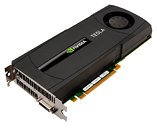
NVIDIA Corporation today unveiled the Tesla 20-series of parallel processors for the high performance computing (HPC) market, based on its new generation CUDA processor architecture, codenamed "Fermi".

Designed from the ground-up for parallel computing, the NVIDIA Tesla 20-series GPUs slash the cost of computing by delivering the same performance of a traditional CPU-based cluster at one-tenth the cost and one-twentieth the power.
The Tesla 20-series introduces features that enable many new applications to perform dramatically faster using GPU Computing. These include ray tracing, 3D cloud computing, video encoding, database search, data analytics, computer-aided engineering and virus scanning.

"NVIDIA has deployed a highly attractive architecture in Fermi, with a feature set that opens the technology up to the entire computing industry," said Jack Dongarra, director of the Innovative Computing Laboratory at the University of Tennessee and co-author of LINPACK and LAPACK.

The Tesla 20-series GPUs combine parallel computing features that have never been offered on a single device before. These include:
  • Support for the next generation IEEE 754-2008 double precision floating point standard
  • ECC (error correcting codes) for uncompromised reliability and accuracy
  • Multi-level cache hierarchy with L1 and L2 caches
  • Support for the C++ programming language
  • Up to 1 terabyte of memory, concurrent kernel execution, fast context switching, 10x faster atomic instructions, 64-bit virtual address space, system calls and recursive functions
At their core, Tesla GPUs are based on the massively parallel CUDA computing architecture that offers developers a parallel computing model that is easier to understand and program than any of the alternatives developed over the last 50 years.

"There can be no doubt that the future of computing is parallel processing, and it is vital that computer science students get a solid grounding in how to program new parallel architectures," said Dr. Wen-mei Hwu, Professor in Electrical and Computer Engineering of the University of Illinois at Urbana-Champaign. "GPUs and the CUDA programming model enable students to quickly understand parallel programming concepts and immediately get transformative speed increases."

The family of Tesla 20-series GPUs includes:
  • Tesla C2050 & C2070 GPU Computing Processors
  • Single GPU PCI-Express Gen-2 cards for workstation configurations
  • Up to 3GB and 6GB (respectively) on-board GDDR5 memory
  • Double precision performance in the range of 520GFlops - 630 GFlops
  • Tesla S2050 & S2070 GPU Computing Systems
  • Four Tesla GPUs in a 1U system product for cluster and datacenter deployments
  • Up to 12 GB and 24 GB (respectively) total system memory on board GDDR5 memory
  • Double precision performance in the range of 2.1 TFlops - 2.5 TFlops
The Tesla C2050 and C2070 products will retail for $2,499 and $3,999 and the Tesla S2050 and S2070 will retail for $12,995 and $18,995. Products will be available in Q2 2010. For more information about the new Tesla 20-series products, visit the Tesla product pages.

As previously announced, the first Fermi-based consumer (GeForce) products are expected to be available first quarter 2010.
Add your own comment

53 Comments on New NVIDIA Tesla GPUs Reduce Cost Of Supercomputing By A Factor Of 10

#26
Zubasa
BenetanegiaThe free AMD video transcoding application, I guess. In it's first itterations was extremely buggy and useless, because it produced massive artifacts on videos. I have not heard since, so I don't know it it has improved.

PD. I don't even know for sure if it's that TBH. :laugh:
Its not that PoS.
I wouldn't touch that Avivo transcoder with a 10 foot pole, don't tempt me :laugh:

Edit: you temped to download that thing lol :roll:
Interesting enough that PoS finally does what it claims to do, it actually loads the GPU @11~17% in pulses.
Posted on Reply
#27
[H]@RD5TUFF
ZubasaYou better hope its not Q3 by the way the 40nm yeilds look :shadedshu
Your speaking of the laughable article written by the giant tool Charlie Demerjian ( www.semiaccurate.com/2009/09/15/nvidia-gt300-yeilds-under-2/ ) even if it is true, it's far from uncommon for early fab results to be poor. It happen to all MC companies ( microcircuitry ) . Years back in 1995 I can remember hearing tell of AMD's K5 ( en.wikipedia.org/wiki/AMD_K5 ) processors reaching a all time low fab rate of of 2 out of a 250 fab wafer! Let alone the fact they were basically just reengineered Pentiums . ZOMG that's less than 1% lets write an article about it! Lets continue to the complete lack of creditability and objectivity Charlie Demerjian has. The essence of what I am saying is, he write articles that rarely cite any fact, and contain little more than jaded, pessimistic, and unobjective opinion.
Posted on Reply
#28
Zubasa
[H]@RD5TUFFYour speaking of the laughable article written by the giant tool Charlie Demerjian ( www.semiaccurate.com/2009/09/15/nvidia-gt300-yeilds-under-2/ ) even if it is true, it's far from uncommon for early fab results to be poor. It happen to all MC companies ( microcircuitry ) . Years back in 1995 I can remember hearing tell of AMD's K5 ( en.wikipedia.org/wiki/AMD_K5 ) processors reaching a all time low fab rate of of 2 out of a 250 fab wafer! Let alone the fact they were basically just reengineered Pentiums . ZOMG that's less than 1% lets write an article about it! Lets continue to the complete lack of creditability and objectivity Charlie Demerjian has. The essence of what I am saying is, he write articles that rarely cite any fact, and contain little more than jaded, pessimistic, and unobjective opinion.
I have never read that site to be honest. :slap:
It is common sense to know that the 40nm yields are not good, simply by looking at the supply (or the lack) of the 5800 series.
Posted on Reply
#29
[H]@RD5TUFF
ZubasaI have never read that site to be honest. :slap:
It is common sense to know that the 40nm yields are not good, simply by looking at the supply (or the lack) of the 5800 series.
The lack of 5800's is due more to the fact AMD's fab / manufacturing, are separate entities / companies, and while it cuts costs, and kept AMD out of bankruptcy. But prevents them from producing their high end products in any large quantities. Hence their budget minded approach to sales, it really isn't a choice, it's all they can do, to keep money in their coffers, and hope to expand come 2012. Their other choice is to try to compete directly with intel, and fade even faster into irrelevance, well faster than they are now anyway. :slap:
Posted on Reply
#30
Zubasa
[H]@RD5TUFFThe lack of 5800's is due more to the fact AMD's fab / manufacturing, are separate entities / companies, and while it cuts costs, and kept AMD out of bankruptcy. But prevents them from producing their high end products in any large quantities. Hence their budget minded approach to sales, it really isn't a choice, it's all they can do, to keep money in their coffers, and hope to expand come 2012. Their other choice is to try to compete directly with intel, and fade even faster into irrelevance, well faster than they are now anyway. :slap:
First of all, AMD don't own any Fabs anymore, and their Graphics were never manufactured in their Fabs. :pimp:

It is TSMC that makes their graphics chips, and it is the same comapny that makes graphics chips for nVidia.:slap:
The actual cards are make by their AIBs, companies like Sapphire (PC Partner) are the ones that actually make the cards.

AMD is a fabless company just like nVidia is now.
Globalfoundries and their Fabs were never invloved.:pimp:

What can be tell from this is, the Fermi's larger die size won't make their yields any better than the Cypress.
So unless TSMC gets their yields up, don't expect a sufficient supply of Fermi(s).
Posted on Reply
#31
W1zzard
PP MguireThis is proof there is a gt300. So where is our desktop cards huh nvidia?
proof that they took a photo of something and wrote a press release
edit: it's not even a photo .. it's rendered not
kid41212003The card can use up to 1TB of system memory?
afaik it means that the gpu architecture is able to address up to 1 tb of memory .. like 32-bit -> 64-bit
Posted on Reply
#32
PP Mguire
I just read q2 and thats when most all of us are expecting 300. Guess i shoulda read a little more Me ->:slap:<- me
Posted on Reply
#33
3volvedcombat
wow they finnaly HAVE A WORKING MODEL OF THERE NEW CORE THIS MEANS THAT HOPEFULLY THE WORLD WILL SEE SOME FERMI SLAPED INTO THE WORLD >.<.

*ATI Lol's while they release HD 5870x2 and have all the shares on there highest end series while everybody goes broke for shiat*
Posted on Reply
#34
erocker
*
BenetanegiaThe free AMD video transcoding application, I guess. In it's first itterations was extremely buggy and useless, because it produced massive artifacts on videos. I have not heard since, so I don't know it it has improved.

PD. I don't even know for sure if it's that TBH. :laugh:
I use it all the time for YouTube stuff. MPEG-2 720p works great, since 9.8's anyways.
Posted on Reply
#36
PP Mguire
With 2 GPUs. I think somebody is BSing somewhere.
Posted on Reply
#37
Benetanegia
kid41212003forums.techpowerup.com/showpost.php?p=1638012&postcount=14

The ratio between single and double precision performance is ~0.083
And :

No one surprise that this card single precision performance is ~4.7 TFLOPS!? (570GFLOPS*0.083)

forums.techpowerup.com/showpost.php?p=1638260&postcount=114

And HD5970 has the same compute performance!

>.>
The ratio in Fermi is 0.5, so these Tesla cards will have 1040-1260 single precision Gflops. Don't let the "low" number fool you anyway, these Fermi cards will trounce the Ati cards when it comes to general computing.

Don't let the numbers fool you in comparison to GTX285 or Ati cards either, GTX285 numbers are based on dual-issue, something that was never usable, real FP was more like 650 Gflops on the GTX285. Nvidia/Ati Gflops numbers don't correlate either, if 650 Gflps GTX285 is still significantly faster than the 1360 Gflops HD4890, the Fermi with 1260 is going to be significantly faster than the 2700 GFlops HD5870. Tesla cards are usually underclocked in comparison to desktop GPUs AFAIK, so this 520-630 DP numbers on the teslas could be the testimony of the power of the GTX380.
Posted on Reply
#38
Zubasa
BenetanegiaThe ratio in Fermi is 0.5, so these Tesla cards will have 1040-1260 single precision Gflops. Don't let the "low" number fool you anyway, these Fermi cards will trounce the Ati cards when it comes to general computing.

Don't let the numbers fool you in comparison to GTX285 or Ati cards either, GTX285 numbers are based on dual-issue, something that was never usable, real FP was more like 650 Gflops on the GTX285. Nvidia/Ati Gflops numbers don't correlate either, if 650 Gflps GTX285 is still significantly faster than the 1360 Gflops HD4890, the Fermi with 1260 is going to be significantly faster than the 2700 GFlops HD5870. Tesla cards are usually underclocked in comparison to desktop GPUs AFAIK, so this 520-630 DP numbers on the teslas could be the testimony of the power of the GTX380.
We don't know what kind of architechure the Fermi is built on anayways.
It is still too early to say before we even see a Engineering Sample in action.

If nVidia somehow and for some reason go for a SIMD architecture, the theoretical limit will sky rocket just like the RV7X0. :rolleyes:
All we have are some vague numbers that doesn't mean too much yet.

It is well possible that the Fermi is more optimized in GPGPU than its predecessors, afterall this is where the big bucks are.
I am more interested in the Graphics performance of a GPU, but this thread is about the new Tesla so I guess I am off topic.
Posted on Reply
#39
@RaXxaa@
Way too overpriced, sure its godd but for gaming seriously i would never pay couple of Gs for a GPU... Sure even in crysis some tesla gives maybe 350 fps but plzz i would buy a gpu that can just give me 35 fps thats it good enough gaming for me
Posted on Reply
#40
Yukikaze
maq_pakiWay too overpriced, sure its godd but for gaming seriously i would never pay couple of Gs for a GPU... Sure even in crysis some tesla gives maybe 350 fps but plzz i would buy a gpu that can just give me 35 fps thats it good enough gaming for me
Of course, Tesla GPUs have nothing to do with gaming.
Posted on Reply
#41
Benetanegia
ZubasaWe don't know what kind of architechure the Fermi is built on anayways.
It is still too early to say before we even see a Engineering Sample in action.
If nVidia somehow and for some reason go for a SIMD architecture, the theoretical limit will sky rocket just like the RV7X0. :rolleyes:
We do know the architecture. White papers have been out for long, architecture is more scalar than it ever was. Nvidia has always used SIMD architecture anyway, but they have not used 5 ALU wide VLIW shader processors. That's the biggest lie AMD has ever made, they have really only 160 SPs on the RV770. That's the "problem" in Ati cards, the effective Gflops on the HD4870 ranges between 1200 and 240 Gflops single precision because of that, depending on how many ALUs-per-SP can be used in a certain scenario. In a general computing application you will be closer to the low end and that's why in F@H you can see Nvidia cards topping out Ati cards that are suposed to be much faster.
Posted on Reply
#42
Zubasa
BenetanegiaWe do know the architecture. White papers have been out for long, architecture is more scalar than it ever was. Nvidia has always used SIMD architecture anyway, but they have not used 5 ALU wide VLIW shader processors. That's the biggest lie AMD has ever made, they have really only 160 SPs on the RV770. That's the "problem" in Ati cards, the effective Gflops on the HD4870 ranges between 1200 and 240 Gflops single precision because of that, depending on how many ALUs-per-SP can be used in a certain scenario. In a general computing application you will be closer to the low end and that's why in F@H you can see Nvidia cards topping out Ati cards that are suposed to be much faster.
Well the Shader processor count is more marketing than anything.
The thing is out of 100 people, how many know what a "5 ALU wide VLIW SP" means?
Very very few companies are totally honest in marketing.
White paper tells you what a product is suppose to do, but it won't tell you how exactly it executes them in the hardware level.
The specific design of the chip is worth millions if not billions of dollars.

Since you mentioned the GTX380, GPGPU performance don't directly transfers to gamming performance.
Posted on Reply
#43
HalfAHertz
BenetanegiaWe do know the architecture. White papers have been out for long, architecture is more scalar than it ever was. Nvidia has always used SIMD architecture anyway, but they have not used 5 ALU wide VLIW shader processors. That's the biggest lie AMD has ever made, they have really only 160 SPs on the RV770. That's the "problem" in Ati cards, the effective Gflops on the HD4870 ranges between 1200 and 240 Gflops single precision because of that, depending on how many ALUs-per-SP can be used in a certain scenario. In a general computing application you will be closer to the low end and that's why in F@H you can see Nvidia cards topping out Ati cards that are suposed to be much faster.
You're trying to compare the SPs to x86 cores, and the two are obviously not compatible...If you do indeed want to do so, you must at least say that those 800 "cores" consist of 160 phisical and 640 logical ones. And that would still be wrong because you don't have a dedicated pipeline that has to be filled for a second or third tread to be inserted...You can still run 800 "threads" on them as long as your software is coded properly.

It's not Ati's fault the F@H team can't put their thinking caps on and write a half-decent client program...
Posted on Reply
#44
wolf
Better Than Native
Yum Yum Fermi, if this is going to be the length of the GeForce card, watch out ATi, 13.5 inches of Dual GPU to to toe to toe with this slim baby.
Posted on Reply
#45
vaiopup
HalfAHertzIt's not Ati's fault the F@H team can't put their thinking caps on and write a half-decent client program...
They've had long enough :D
Posted on Reply
#46
Benetanegia
HalfAHertzYou're trying to compare the SPs to x86 cores, and the two are obviously not compatible...If you do indeed want to do so, you must at least say that those 800 "cores" consist of 160 phisical and 640 logical ones. And that would still be wrong because you don't have a dedicated pipeline that has to be filled for a second or third tread to be inserted...You can still run 800 "threads" on them as long as your software is coded properly.

It's not Ati's fault the F@H team can't put their thinking caps on and write a half-decent client program...
Nope that's the case. There's only 160 pipelines, so you can have 160 threads feeding those 800 "cores" as long as the program can pack them together in an VLIW instruction, but it's not exactly the same and requires a lot of anticipation, not always posible. In fact almost never posible.

I'm not compating the SPs to x86 cores in any way, I don't know how did you come up to that conclusion.

Because of the VLIW nature of the SPs you could potentially make an engine that only works with 5 wide VLIW instructions and then you could potentially fill all the "cores", but that engine would not work on Nvidia cards or pre R600 Ati cards, not to mention it would not be profitable to do so and DirectX has no such functionality so you would have to make your engine entirely on HLSL. Still filling the 5 ALUs with something relevant to do would be very very difficult.

perspectives.mvdirona.com/2009/03/18/HeterogeneousComputingUsingGPGPUsAMDATIRV770.aspx
Unlike NVidia’s design which executes 1 instruction per thread, each SP on the RV770 executes packed 5-wide VLIW-style instructions. For graphics and visualization workloads, floating point intensity is high enough to average about 4.2 useful operations per cycle. On dense data parallel operations (ex. dense matrix multiply), all 5 ALUs can easily be used.
From this information, we can see that when people are talking about 800 “shader cores” or “threads” or “streaming processors”, they are actually referring to the 10*16*5 = 800 xyzwt ALUs. This can be confusing, because there are really only 160 simultaneous instruction pipelines.
On general computing you will not see that typical usage of 4.2 and will be closer to 1 most times than not and hence the real Gflops on the Ati cards with this design is 1/5th or 2/5th of the peak throughoutput.

Also when a special function must be calculated you loose one of those ALUs (the fat one) for many clocks (probably you loose the entire SP), whereas the Nvidia card can do both the SF and the ALU operation and this is not the famous dual-issue, it can always be done as long as the SF function and the thread being executed in the ALUs were issued in a different clock.
Posted on Reply
#48
HalfAHertz
BenetanegiaNope that's the case. There's only 160 pipelines, so you can have 160 threads feeding those 800 "cores" as long as the program can pack them together in an VLIW instruction, but it's not exactly the same and requires a lot of anticipation, not always posible. In fact almost never posible.

I'm not compating the SPs to x86 cores in any way, I don't know how did you come up to that conclusion.

Because of the VLIW nature of the SPs you could potentially make an engine that only works with 5 wide VLIW instructions and then you could potentially fill all the "cores", but that engine would not work on Nvidia cards or pre R600 Ati cards, not to mention it would not be profitable to do so and DirectX has no such functionality so you would have to make your engine entirely on HLSL. Still filling the 5 ALUs with something relevant to do would be very very difficult.

perspectives.mvdirona.com/2009/03/18/HeterogeneousComputingUsingGPGPUsAMDATIRV770.aspx


On general computing you will not see that typical usage of 4.2 and will be closer to 1 most times than not and hence the real Gflops on the Ati cards with this design is 1/5th or 2/5th of the peak throughoutput.

Also when a special function must be calculated you loose one of those ALUs (the fat one) for many clocks (probably you loose the entire SP), whereas the Nvidia card can do both the SF and the ALU operation and this is not the famous dual-issue, it can always be done as long as the SF function and the thread being executed in the ALUs were issued in a different clock.
For graphics and visualization workloads, floating point intensity is high enough to average about 4.2 useful operations per cycle
I don't want to derail the toppic, but on general computing, you will see the benefit if you're using the simpler single precision calculations, you may not see the benefit if you are using double tho.
Also, both NVidia and AMD use symmetric single issue streaming multiprocessor architectures, so branches are handled very differently from CPUs.
You were right here tho. There is a single pipeline but it doesn't hve to be flooded for a second thread to be loaded! :)

That was a really insightful article, thanks. Still what I was trying to say was that if there's a will, there's always a way. As you said it yourself, you need to code specifically for ati's architecture and that could mean a seperate executable. I'm not saying that game companies should invest their own time and money to code a game specifically for ati users, no they shoudn't. If ati wants to have better support for their cards, they should sponsor game manufacturers just like nvidia does. Still there is nothing stopping a non-profit organisation like F@H to actually try and use all that computing power avaible to them...
Posted on Reply
#49
Benetanegia
HalfAHertz

I don't want to derail the toppic, but on general computing, you will see the benefit if you're using the simpler single precision calculations, you may not see the benefit if you are using double tho.
That depends entirely on how linear* the code is. On graphics you can always use most of the shaders, because data is parallel enough as well as istruction type is parallel enough. In general computing is quite the oposite and although the chip might be able to run all that code in parallel in theory, aka there's no physical limitation onto it, there is a limitation in the code itself, and not because of the lack of optimization, but because of the nature of the code, because of the self dependencies. A lot has been discussed on the CPUs about this too, that the programers are lazy in not implemeting their code for multi-cores, but reality is that a lot of code simply can't be split into many threads.

A lot can be said about a bus with 50 seats being a more efficient and powerful way of transportation than a mini-bus with 12 seats, but if your working flow is go to town A -> take up 10 people -> go to B -> 10 people down/another 10 up -> go to C -> 10 leave/10 up and so on, your 50 seat bus is much less efficient than the mini-bus, and there's very little you can do about that. And there's very little the passengers (=software) can do on their front too.

* I'm talking about the ILP (Instruction Level Parallelism) and TLP (Thread level) both at the same time. Ati architecture needs both to be effective (because SIMD+VLIW) and that's a luxury you will not find in general computing quite often.
Posted on Reply
#50
[I.R.A]_FBi
PP MguireThis is proof there is a gt300. So where is our desktop cards huh nvidia?
As previously announced, the first Fermi-based consumer (GeForce) products are expected to be available first quarter 2010.

;)
Posted on Reply
Add your own comment
Nov 29th, 2024 06:48 EST change timezone

New Forum Posts

Popular Reviews

Controversial News Posts