Thursday, June 19th 2014

NVIDIA GeForce GTX 880 and GTX 870 to Launch This Q4

NVIDIA is planning to launch its next high performance single-GPU graphics cards, the GeForce GTX 880 and GTX 870, no later than Q4-2014, in the neighborhood of October and November, according to a SweClockers report. The two will be based on the brand new "GM204" silicon, which most reports suggest, is based on the existing 28 nm silicon fab process. Delays by NVIDIA's principal foundry partner TSMC to implement its next-generation 20 nm process has reportedly forced the company to design a new breed of "Maxwell" based GPUs on the existing 28 nm process. The architecture's good showing with efficiency on the GeForce GTX 750 series probably gave NVIDIA hope. When 20 nm is finally smooth, it wouldn't surprise us if NVIDIA optically shrinks these chips to the new process, like it did to the G92 (from 65 nm to 55 nm). The GM204 chip is rumored to feature 3,200 CUDA cores, 200 TMUs, 32 ROPs, and a 256-bit wide GDDR5 memory interface. It succeeds the company's current workhorse chip, the GK104.
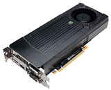
Source: SweClockers
Add your own comment

72 Comments on NVIDIA GeForce GTX 880 and GTX 870 to Launch This Q4

#2
XSI
I would be happy to change my 8800GT to GTX 880 :)
Posted on Reply
#3
The Von Matrices
btarunrWhen 20 nm is finally smooth, it wouldn't surprise us if NVIDIA optically shrinks these chips to the new process, like it did to the G92 (from 65 nm to 55 nm).
I have to disagree with you here. 20nm isn't going to be less expensive than 28nm per transistor, so there's no financial incentive for a die shrink and thus it won't be done. It makes more financial sense to sell a large 28nm chip than a smaller 20nm chip.

20nm will only be for the extreme high end this generation and will only be used in cases where it's impossible to manufacture a larger 28nm chip (e.g. you can't make a 28nm, 15 billion transistor, 1100mm^2 GM100). 20nm won't become mainstream until NVidia (or anyone else) can't achieve their performance targets on 28nm, which likely will not happen until the generation after this.
Posted on Reply
#4
GreiverBlade
btarunrThe GM204 chip is rumored to feature 3,200 CUDA cores, 200 TMUs, 32 ROPs, and a 256-bit wide GDDR5
i can't wait to see how a 880 does against 780/780Ti R9 290/290X ... if the gain is minimal (15-25%) and the tdp is the major point: then no regrets. :D (specially if Nv does the pricing "à la nVidia")
Posted on Reply
#5
THE_EGG
Earlier than I thought. I thought it would be coming out around December 2014 to February 2015 sometime. Looking forward to it!
Posted on Reply
#6
MxPhenom 216
ASIC Engineer
I expect GM210, big die Maxwell to debut 20nm.
Posted on Reply
#7
ZoneDymo
Will be interesting to see how it preforms, will it handle 4k good enough etc, and power usage.
But that 28nm v 20nm makes it feel like an inbetween thing you dont want imo.
Posted on Reply
#8
alwayssts
d1nkyalready?!
LOL...
___

I don't understand why people think a 256-bit/32 ROP chip is going to have something like 3200sp. That makes absolutely no sense. Half that (according to nvidia-speak), at most, is feasible.

One of those components, at least, is wrong. It could be 256-bit/32 ROPs/1536(1920), or given since we know it is 8GB (and sixteen 4GB chips is a lot for a mid-range part), 512-bit/64/3200, or some combo of more cache/256-bit/64 ROPs/3200 because the design probably will indeed likely be shrank to 20nm where size will prohibit a larger bus. You gotta remember 3200sp, or 25 SMM, is essentially similar to 4000sp from AMD. That's a lot of chip, more than actually needed for 64 ROPs on avg (where-as Hawaii would be optimal for 48, if the design allowed it)...and again if true we can probably more realistically expect 23-24 (3072) unit parts, as it makes the most efficient sense. Not unlike Titan, for instance, and the full design is probably a safety net.

I agree it will be shrank, but I think a more suitable comparison would be G80->G92b...because if accurate we're talking a huge chip (~4x gm107) transitioning to a process that's supposed to allow somewhere around 1.9x density, granted around 1.2-1.3x performance/power savings. That means going from behemoth size (GT200 was 576mm) to large 256-bit size (like GK104 which is 294mm, and probably the largest really feasible before being larger and switching to a larger controller with slower ram). I certainly see how it could be conceivable to have such a large design on 28nm, and then scale size down and clockspeed up as we move to newer processes. That doesn't necessarily mean it's market will change...a small(ish) chip on 20nm/16nm (20nmFF) will likely be very expensive, but the clock improvement/power savings could, at least in on the later, make the change worth it.

I'm really curious how they could get a 3072sp (equivalent to 3840sp from amd) with 8GB of ram within a decent power envelope, especially in a feasible manner (meaning at least .9v and around 876mhz, the minimum voltage for the process and avg clocks at that voltage). I don't doubt the design is 'possible', especially with low-speed/voltage and higher density ram on a smaller bus (cache is probably more power efficient), but damn....that's pushing it to the edge of feasibility on pretty much all counts.
Posted on Reply
#9
Dejstrum
Finally....... I need to change my gtx 570
Posted on Reply
#10
RCoon
Alright, I don't expect any miracles then. Same process, but more cores? It's just Kepler with 400 more cores on a slightly more energy efficient architecture. So they might deal with the heat increase by adding more cores by using the slightly more efficient archi, and in turn gain a small performance increase from 2880 cores to 3200. I'm assuming the 870 will have ~3000 cores to hit a price point between the two.

Call me cynical, but I don't see the 780ti lowering in price and the 880 taking its place. The 880 is going to hit a higher price point. Then there's the simple fact that the 860 is probably going to just be a rebranded 780ti and everything else below will likely be a rebrand too. Ugh... new GPU releases are so disappointing these days... nothing to get excited about, especially when you know the price gouging is imminent.
Posted on Reply
#11
arbiter
RCoonAlright, I don't expect any miracles then. Same process, but more cores? It's just Kepler with 400 more cores on a slightly more energy efficient architecture. So they might deal with the heat increase by adding more cores by using the slightly more efficient archi, and in turn gain a small performance increase from 2880 cores to 3200. I'm assuming the 870 will have ~3000 cores to hit a price point between the two.
Sighting more efficient? you should check on 750ti and see how its power usage compares. It used less then 50% the power 650ti used, yea 650ti had 768 cores and 750ti only had 640. 650 non-ti had 384 cores and it used 4 more watts then 750ti was rated it. I don't expect it to be 50% of what 780's use which is listed around 250 watts but very possible it could be around ~150-175watt range maybe little higher.
Posted on Reply
#12
The Von Matrices
alwaysstsdon't understand why people think a 256-bit/32 ROP chip is going to have something like 3200sp. That makes absolutely no sense. Half that (according to nvidia-speak), at most, is feasible.

One of those components, at least, is wrong. It could be 256-bit/32 ROPs/1536(1920), or given since we know it is 8GB (and sixteen 4GB chips is a lot for a mid-range part), 512-bit/64/3200, or some combo of more cache/256-bit/64 ROPs/3200 because the design probably will indeed likely be shrank to 20nm where size will prohibit a larger bus. You gotta remember 3200sp, or 25 SMM, is essentially similar to 4000sp from AMD. That's a lot of chip, more than actually needed for 64 ROPs on avg (where-as Hawaii would be optimal for 48, if the design allowed it)...and again if true we can probably more realistically expect 23-24 (3072) unit parts, as it makes the most efficient sense. Not unlike Titan, for instance, and the full design is probably a safety net.

I agree it will be shrank, but I think a more suitable comparison would be G80->G92b...because if accurate we're talking a huge chip (~4x gm107) transitioning to a process that's supposed to allow somewhere around 1.9x density, granted around 1.2-1.3x performance/power savings. That means going from behemoth size (GT200 was 576mm) to large 256-bit size (like GK104 which is 294mm, and probably the largest really feasible before being larger and switching to a larger controller with slower ram). I certainly see how it could be conceivable to have such a large design on 28nm, and then scale size down and clockspeed up as we move to newer processes. That doesn't necessarily mean it's market will change...a small(ish) chip on 20nm/16nm (20nmFF) will likely be very expensive, but the clock improvement/power savings could, at least in on the later, make the change worth it.

I'm really curious how they could get a 3072sp (equivalent to 3840sp from amd) with 8GB of ram within a decent power envelope, especially in a feasible manner (meaning at least .9v and around 876mhz, the minimum voltage for the process and avg clocks at that voltage). I don't doubt the design is 'possible', especially with low-speed/voltage and higher density ram on a smaller bus (cache is probably more power efficient), but damn....that's pushing it to the edge of feasibility on pretty much all counts.
I think the much simpler explanation is the one that Cadaveca posted at the last leak. The different SKUs are getting mixed up and 3200SP and 8GB is for a dual-GPU card, the successor to GTX 690. The single GPU part, successor to the GTX 680/GTX 770 would therefore have 4GB and 1600SP. To me, this is much more reasonable.

Remember, GTX 750 Ti outperforms the GTX 650 Ti by 20% and yet it has 20% fewer shaders, so assuming the same scaling, a 1600SP GTX 880 would have almost 50% more performance than GTX 770/680, completely in line with a generational improvement.

Edit: updated correct card names
Posted on Reply
#13
RCoon
arbiterSighting more efficient? you should check on 750ti and see how its power usage compares. It used less then 50% the power 650ti used, yea 650ti had 768 cores and 750ti only had 640. 650 non-ti had 384 cores and it used 4 more watts then 750ti was rated it. I don't expect it to be 50% of what 780's use which is listed around 250 watts but very possible it could be around ~150-175watt range maybe little higher.
Yeah I understand the 750ti was a total baller for energy efficiency, but it wasn't just down to cores. This 880 has more of everything, wider memory bus, etc, so while it will undoubtedly use less power than the 780ti, I don't forsee it being a massive amount, like you said, the difference of 250W and 175W, I reckon ~50W or more in savings sounds about right.
Posted on Reply
#14
techy1
will it run Crysis in 4K? if the answer is "no" - why should we bother and even talk about this useless hardware. if the answer is "yes" - then shut up and take my money
Posted on Reply
#15
HumanSmoke
The Von MatricesI have to disagree with you here. 20nm isn't going to be less expensive than 28nm per transistor, so there's no financial incentive for a die shrink and thus it won't be done. It makes more financial sense to sell a large 28nm chip than a smaller 20nm chip.
It does make financial sense to go with 28nm, but I doubt it is because of the reason you've given.
Transistor density for 20nm (16nm FEOL + 20m BEOL) isestimated at 1.9 - 2.0x that of 28nm.
Wafer costs: 28nm : $4500-5000 per. 20nm: $6000 per....1.3x that of 28nm.

Reasons to go with 28nm?
Available capacity
Yields
Would the GPU design benefit from, or require increased transistor density over increased GPU silicon cost for the given price points of the product being sold? The GTX 870/880 (and presumably followed by the GTX 860 Ti) would still likely reside in the $350/$500 segment brackets. Why add to the manufacturing cost when you're under no pressure to do so (since AMD will also go with 28nm for their next iteration of GPUs).

My guess is that neither Nvidia nor AMD trust TSMC to deliver a large IC in commercial quantity based on TSMC's projections. Given the woes of 32nm and the slow and problematic ramp of 28nm who could blame them?
Posted on Reply
#16
Squuiid
What I most want to know is do these cards do HDMI 2.0 and Displayport 1.3?
Until both video cards and 4K monitors support BOTH of these standards I won't be dumping my GTX590 any time soon.
These two standards are a must for 4K IMO.
Posted on Reply
#17
Roel
I am hoping for cards with 3 DisplayPort connections.
Posted on Reply
#18
FrustratedGarrett
arbiterSighting more efficient? you should check on 750ti and see how its power usage compares. It used less then 50% the power 650ti used, yea 650ti had 768 cores and 750ti only had 640. 650 non-ti had 384 cores and it used 4 more watts then 750ti was rated it. I don't expect it to be 50% of what 780's use which is listed around 250 watts but very possible it could be around ~150-175watt range maybe little higher.
Yeah but the the Maxwell GM107 is ~160mm^2 and it only packs half the performance of the GK104 which measures ~300mm^2, so Maxwell doesn't improve efficiency area wise. I expect the new chips to be big, and while not as power hungry as the GK110 chips, performance is not going to be much better.

BTW, I think the 3200 CUDA cores is impossible. If GM107 can pack 640 CUDA cores onto a ~160mm^2 chip, then a 450mm^2 chip can't pack more than ~2000 cores.
I
expect 15%-20% better performance than the 780TI at lower prices, which is great nevertheless!
Posted on Reply
#19
The Von Matrices
HumanSmokeIt does make financial sense to go with 28nm, but I doubt it is because of the
reason you've given.
Transistor density for 20nm (16nm FEOL + 20m BEOL) isestimated at 1.9 - 2.0x that of 28nm.
Wafer costs: 28nm : $4500-5000 per. 20nm: $6000 per....1.3x that of 28nm.

Reasons to go with 28nm?
Available capacity
Yields
Would the GPU design benefit from, or require increased transistor density over increased GPU silicon cost for the given price points of the product being sold? The GTX 870/880 (and presumably followed by the GTX 860 Ti) would still likely reside in the $350/$500 segment brackets. Why add to the manufacturing cost when you're under no pressure to do so (since AMD will also go with 28nm for their next iteration of GPUs).

My guess is that neither Nvidia nor AMD trust TSMC to deliver a large IC in commercial quantity based on TSMC's projections. Given the woes of 32nm and the slow and problematic ramp of 28nm who could blame them?
I should clarify my point. I was making my comment based upon NVidia's own press slide showing the transition to cost-effective 20nm occurring in Q1 2015.


The difference in cost per transistor between 20nm and 28nm is minimal, making me question whether it's worth putting engineering effort toward shrinking GPUs for a marginal cost savings per GPU (that may never make up the capital expenditure to make new masks and troubleshoot issues) rather than concentrating engineering on completely new GPUs at that smaller process. Unlike in the past, there's a lot more to be gained from a newer, more efficient architecture than from a die shrink.
Posted on Reply
#20
RejZoR
People still obsessed with stupid power consumption. Its like buying a Ferrari and then driving around at 50km/h to conserve petrol. Or worse, driving a Ferrari and constantly bitch about MPG. Idiotic. Give me cheaper top performing card and i don't give a toss about consumption.
Posted on Reply
#21
Constantine Yevseyev
techy1will it run Crysis in 4K? if the answer is "no" - why should we bother and even talk about this useless hardware. if the answer is "yes" - then shut up and take my money
Dude, you have so much to learn about computer software, I don't even know where you should start...
Posted on Reply
#22
robert3892
ZoneDymoWill be interesting to see how it preforms, will it handle 4k good enough etc, and power usage.
But that 28nm v 20nm makes it feel like an inbetween thing you dont want imo.
I don't think you'll see good 4K support until 2015
Posted on Reply
#23
Keullo-e
S.T.A.R.S.
I'll just guess that the full GM204 has 2560 shaders.
Posted on Reply
#24
HumanSmoke
FrustratedGarrettYeah but the the Maxwell GM107 is ~160mm^2 and it only packs half the performance of the GK104 which measures ~300mm^2, so Maxwell doesn't improve efficiency area wise.
GM107 is 148mm², GK104 is 294mm².
You can say that the Maxwell is half the size for slightly better than half the performance, although the comparison is somewhat flawed since the Maxwell chip is hampered by a constrained bus width, and the Maxwell chip devotes a larger percentage of its die area in comparison to GK104 to its uncore (the L2 cache is a significant increase, but not particularly relevant to gaming at this time).
As you say, I'd be very sceptical over the 3200 core claim. The GM204 is obviously designed to supplant GK104, not GK110.
Posted on Reply
#25
TheDeeGee
techy1will it run Crysis in 4K? if the answer is "no" - why should we bother and even talk about this useless hardware. if the answer is "yes" - then shut up and take my money
Just like "Mom" jokes, the Crysis ones also getting old.

And btw Crysis is a turd that can't be polished.
Posted on Reply
Add your own comment
Apr 19th, 2024 19:36 EDT change timezone

New Forum Posts

Popular Reviews

Controversial News Posts