- Joined
- Aug 19, 2017
- Messages
- 2,654 (0.99/day)
On December 31st, AMD's Radeon group has filed a patent for a chiplet architecture of the GPU, showing its vision about the future of Radeon GPUs. Currently, all of the GPUs available on the market utilize the monolithic approach, meaning that the graphics processing units are located on a single die. However, the current approach has its limitations. As the dies get bigger for high-performance GPU configurations, they are more expensive to manufacture and can not scale that well. Especially with modern semiconductor nodes, the costs of dies are rising. For example, it would be more economically viable to have two dies that are 100 mm² in size each than to have one at 200 mm². AMD realized that as well and has thus worked on a chiplet approach to the design.
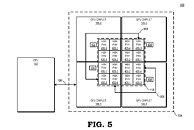
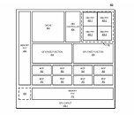
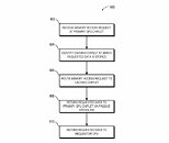
AMD reports that the use of multiple GPU configuration is inefficient due to limited software support, so that is the reason why GPUs were kept monolithic for years. However, it seems like the company has found a way to go past the limitations and implement a sufficient solution. AMD believes that by using its new high bandwidth passive crosslinks, it can achieve ideal chiplet-to-chiplet communication, where each GPU in the chiplet array would be coupled to the first GPU in the array. All the communication would go through an active interposer which would contain many layers of wires that are high bandwidth passive crosslinks. The company envisions that the first GPU in the array would communicably be coupled to the CPU, meaning that it will have to use the CPU possibly as a communication bridge for the GPU arrays. Such a thing would have big latency hit so it is questionable what it means really.
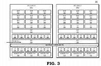
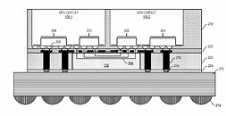
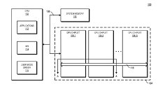
The patent also suggests that each GPU chiplet uses its own Last Level Cache (LLC), instead of separate LLCs for each GPU, so each of the LLCs is communicably coupled and the cache remains coherent across all chiplets. Rumors suggest that we are going to see the first chiplet-based architecture from AMD as successor to the RDNA3 generation, so it will happen in the coming years. AMD already has experience with chiplets from its processors, with Ryzen processors being the prime example. We just need to wait and see how it will look once it arrives for GPUs.
View at TechPowerUp Main Site
AMD reports that the use of multiple GPU configuration is inefficient due to limited software support, so that is the reason why GPUs were kept monolithic for years. However, it seems like the company has found a way to go past the limitations and implement a sufficient solution. AMD believes that by using its new high bandwidth passive crosslinks, it can achieve ideal chiplet-to-chiplet communication, where each GPU in the chiplet array would be coupled to the first GPU in the array. All the communication would go through an active interposer which would contain many layers of wires that are high bandwidth passive crosslinks. The company envisions that the first GPU in the array would communicably be coupled to the CPU, meaning that it will have to use the CPU possibly as a communication bridge for the GPU arrays. Such a thing would have big latency hit so it is questionable what it means really.


The patent also suggests that each GPU chiplet uses its own Last Level Cache (LLC), instead of separate LLCs for each GPU, so each of the LLCs is communicably coupled and the cache remains coherent across all chiplets. Rumors suggest that we are going to see the first chiplet-based architecture from AMD as successor to the RDNA3 generation, so it will happen in the coming years. AMD already has experience with chiplets from its processors, with Ryzen processors being the prime example. We just need to wait and see how it will look once it arrives for GPUs.


View at TechPowerUp Main Site


