- Joined
- Oct 9, 2007
- Messages
- 47,235 (7.55/day)
- Location
- Hyderabad, India
| System Name | RBMK-1000 |
|---|---|
| Processor | AMD Ryzen 7 5700G |
| Motherboard | ASUS ROG Strix B450-E Gaming |
| Cooling | DeepCool Gammax L240 V2 |
| Memory | 2x 8GB G.Skill Sniper X |
| Video Card(s) | Palit GeForce RTX 2080 SUPER GameRock |
| Storage | Western Digital Black NVMe 512GB |
| Display(s) | BenQ 1440p 60 Hz 27-inch |
| Case | Corsair Carbide 100R |
| Audio Device(s) | ASUS SupremeFX S1220A |
| Power Supply | Cooler Master MWE Gold 650W |
| Mouse | ASUS ROG Strix Impact |
| Keyboard | Gamdias Hermes E2 |
| Software | Windows 11 Pro |
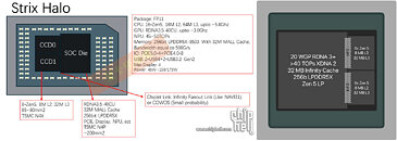
Apparently the AMD "Strix Halo" processor is real, and it's large. The chip is designed to square off against the likes of the Apple M3 Pro and M3 Max, in letting ultraportable notebooks have powerful graphics performance. A chiplet-based processor, not unlike the desktop socketed "Raphael," and mobile BGA "Dragon Range," the "Strix Halo" processor consists of one or two CCDs containing CPU cores, wired to a large die, that's technically the cIOD (client I/O die), but containing an oversized iGPU, and an NPU. The point behind "Strix Halo" is to eliminate the need for a performance-segment discrete GPU, and conserve its PCB footprint.
According to leaks by Harukaze5719, a reliable source with AMD leaks, "Strix Halo" comes in a BGA package dubbed FP11, measuring 37.5 mm x 45 mm, which is significantly larger than the 25 mm x 40 mm size of the FP8 BGA package that the regular "Strix Point," "Hawk Point," and "Phoenix" mobile processors are built on. It is larger in area than the 40 mm x 40 mm FL1 BGA package of "Dragon Range" and upcoming "Fire Range" gaming notebook processors. "Strix Halo" features one or two of the same 4 nm "Zen 5" CCDs featured on the "Granite Ridge" desktop and "Fire Range" mobile processors, but connected to a much larger I/O die, as we mentioned.

At this point, the foundry node of the I/O die of "Strix Halo" is not known, but it's unlikely to be the same 6 nm node as the cIOD that AMD has been using on its other client processors based on "Zen 4" and "Zen 5." It wouldn't surprise us if AMD is using the same 4 nm node as it did for "Phoenix," for this I/O die. The main reason an advanced node is warranted, is because of the oversized iGPU, which features a whopping 20 workgroup processors (WGPs), or 40 compute units (CU), worth 2,560 stream processors, 80 AI accelerators, and 40 Ray accelerators. This iGPU is based on the latest RDNA 3.5 graphics architecture.
For perspective, the iGPU of the regular 4 nm "Strix Point" processor has 8 WGPs (16 CU, 1,024 stream processors). Then there's the NPU. AMD is expected to carry over the same 50 TOPS-capable XDNA 2 NPU it uses on the regular "Strix Point," on the I/O die of "Strix Halo," giving the processor Microsoft Copilot+ capabilities.
The memory interface of "Strix Halo" has for long been a mystery. Logic dictates that it's a terrible idea to have 16 "Zen 5" CPU cores and a 40-Compute Unit GPU share even a regular dual-channel DDR5 memory interface at the highest possible speeds, as both the CPU and iGPU would be severely bandwidth-starved. Then there's also the NPU to consider, as AI inferencing is a memory-sensitive application.
We have a theory, that besides an LPDDR5X interface for the CPU cores, the "Strix Halo" package has wiring for discrete GDDR6 memory. Even a relatively narrow 128-bit GDDR6 memory interface running at 20 Gbps would give the iGPU 320 GB/s of memory bandwidth, which is plenty for performance-segment graphics. This would mean that besides LPDDR5X chips, there would be four GDDR6 chips on the PCB. The iGPU even has 32 MB of on-die Infinity Cache memory, which seems to agree with our theory of a 128-bit GDDR6 interface exclusively for the iGPU.
View at TechPowerUp Main Site | Source
According to leaks by Harukaze5719, a reliable source with AMD leaks, "Strix Halo" comes in a BGA package dubbed FP11, measuring 37.5 mm x 45 mm, which is significantly larger than the 25 mm x 40 mm size of the FP8 BGA package that the regular "Strix Point," "Hawk Point," and "Phoenix" mobile processors are built on. It is larger in area than the 40 mm x 40 mm FL1 BGA package of "Dragon Range" and upcoming "Fire Range" gaming notebook processors. "Strix Halo" features one or two of the same 4 nm "Zen 5" CCDs featured on the "Granite Ridge" desktop and "Fire Range" mobile processors, but connected to a much larger I/O die, as we mentioned.

At this point, the foundry node of the I/O die of "Strix Halo" is not known, but it's unlikely to be the same 6 nm node as the cIOD that AMD has been using on its other client processors based on "Zen 4" and "Zen 5." It wouldn't surprise us if AMD is using the same 4 nm node as it did for "Phoenix," for this I/O die. The main reason an advanced node is warranted, is because of the oversized iGPU, which features a whopping 20 workgroup processors (WGPs), or 40 compute units (CU), worth 2,560 stream processors, 80 AI accelerators, and 40 Ray accelerators. This iGPU is based on the latest RDNA 3.5 graphics architecture.
For perspective, the iGPU of the regular 4 nm "Strix Point" processor has 8 WGPs (16 CU, 1,024 stream processors). Then there's the NPU. AMD is expected to carry over the same 50 TOPS-capable XDNA 2 NPU it uses on the regular "Strix Point," on the I/O die of "Strix Halo," giving the processor Microsoft Copilot+ capabilities.
The memory interface of "Strix Halo" has for long been a mystery. Logic dictates that it's a terrible idea to have 16 "Zen 5" CPU cores and a 40-Compute Unit GPU share even a regular dual-channel DDR5 memory interface at the highest possible speeds, as both the CPU and iGPU would be severely bandwidth-starved. Then there's also the NPU to consider, as AI inferencing is a memory-sensitive application.
We have a theory, that besides an LPDDR5X interface for the CPU cores, the "Strix Halo" package has wiring for discrete GDDR6 memory. Even a relatively narrow 128-bit GDDR6 memory interface running at 20 Gbps would give the iGPU 320 GB/s of memory bandwidth, which is plenty for performance-segment graphics. This would mean that besides LPDDR5X chips, there would be four GDDR6 chips on the PCB. The iGPU even has 32 MB of on-die Infinity Cache memory, which seems to agree with our theory of a 128-bit GDDR6 interface exclusively for the iGPU.
View at TechPowerUp Main Site | Source


