malware
New Member
- Joined
- Nov 7, 2004
- Messages
- 5,422 (0.74/day)
- Location
- Bulgaria
| Processor | Intel Core 2 Quad Q6600 G0 VID: 1.2125 |
|---|---|
| Motherboard | GIGABYTE GA-P35-DS3P rev.2.0 |
| Cooling | Thermalright Ultra-120 eXtreme + Noctua NF-S12 Fan |
| Memory | 4x1 GB PQI DDR2 PC2-6400 |
| Video Card(s) | Colorful iGame Radeon HD 4890 1 GB GDDR5 |
| Storage | 2x 500 GB Seagate Barracuda 7200.11 32 MB RAID0 |
| Display(s) | BenQ G2400W 24-inch WideScreen LCD |
| Case | Cooler Master COSMOS RC-1000 (sold), Cooler Master HAF-932 (delivered) |
| Audio Device(s) | Creative X-Fi XtremeMusic + Logitech Z-5500 Digital THX |
| Power Supply | Chieftec CFT-1000G-DF 1kW |
| Software | Laptop: Lenovo 3000 N200 C2DT2310/3GB/120GB/GF7300/15.4"/Razer |
An innovative and easily implemented technique in which nanoscale elements precisely assemble themselves over large surfaces could soon open doors to dramatic improvements in the data storage capacity of electronic media, according to scientists at the University of California, Berkeley, and the University of Massachusetts Amherst (UMass Amherst).
"I expect that the new method we developed will transform the microelectronic and storage industries, and open up vistas for entirely new applications," said co-lead investigator Thomas Russell, director of the Materials Research Science and Engineering Center at UMass Amherst, visiting Miller Professor at UC Berkeley's Department of Chemistry, and one of the world's leading experts on the behavior of polymers. "This work could possibly be translated into the production of more energy-efficient photovoltaic cells, for instance."

Russell conceived of this new approach with co-lead investigator Ting Xu, a UC Berkeley assistant professor with joint appointments in the Department of Material Sciences and Engineering and the Department of Chemistry. They describe their work in the Feb. 20 issue of the journal Science.
"The density achievable with the technology we've developed could potentially enable the contents of 250 DVDs to fit onto a surface the size of a quarter," said Xu, who is also a faculty scientist at Lawrence Berkeley National Laboratory.
Xu explained that the molecules in the thin film of block copolymers - two or more chemically dissimilar polymer chains linked together - will self-assemble into an extremely precise, equidistant pattern when spread out on a surface, much like a regiment of disciplined soldiers lining up in formation. For more than a decade, researchers have been trying to exploit this characteristic for use in semiconductor manufacturing, but they have been constrained because the order starts to break down as the size of the area increases.
Once the formation breaks down, the individual domains cannot be read or written to, rendering them useless as a form of data storage.
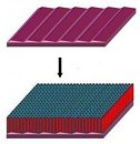
To overcome this size constraint, Russell and Xu conceived of the elegantly simple solution of layering the film of block copolymers onto the surface of a commercially available sapphire crystal. When the crystal is cut at an angle - a common procedure known as a miscut - and heated to 1,300 to 1,500 degrees Centigrade (2,372 to 2,732 degrees Fahrenheit) for 24 hours, its surface reorganizes into a highly ordered pattern of sawtooth ridges that can then be used to guide the self-assembly of the block polymers.
With this technique, the researchers were able to achieve defect-free arrays of nanoscopic elements with feature sizes as small as 3 nanometers, translating into densities of 10 terabits per square inch. One terabit is equal to 1 trillion bits, or 125 gigabytes.
Because crystals come in a variety of sizes, there are few limitations to how large this block copolymer array can be produced, the researchers said. They also noted that the angle and depth of the sawtooth ridges can be easily varied by changing the temperature at which the crystal is heated to fine tune the desired pattern.
"We can generate nearly perfect arrays over macroscopic surfaces where the density is over 15 times higher than anything achieved before," said Russell. "With that order of density, one could get a high-definition picture on a screen the size of a JumboTron."
"It's one thing to get dozens of soldiers to stand in perfect formation in an area the size of a classroom, each person equidistant from the other, but quite another to get tens of trillions of individuals to do so on the field in a football stadium," Xu added. "Using this crystal surface as a guide is like giving the soldiers a marker so they know where to stand."
Other research teams across the country are engaged in similar efforts to break the size barrier of self-assembled block copolymers, but this new project by the UMass Amherst-UC Berkeley scientists differs in that it does not rely upon advances in lithography to achieve its goals.
In the semiconductor industry, optical lithography is a process in which light passes through a mask with a desired circuit pattern onto a photosensitive material, or photoresist, that undergoes a chemical change. Several steps of chemical treatment are then used to develop the desired pattern for subsequent use.
To keep up with Moore's Law and the demand for increasingly smaller features for semiconductors and microprocessors, industry has turned to nanolithography and the use of ever-shorter wavelengths of light at greater cost.
"The challenge with photolithography is that it is rapidly approaching the resolution limits of light," said Xu. "In our approach, we shifted away from this 'top down' method of producing smaller features and instead utilized advantages of a 'bottom up' approach. The beauty of the method we developed is that it takes from processes already in use in industry, so it will be very easy to incorporate into the production line with little cost."
An added benefit, said Xu, is that "our technique is more environmentally friendly than photolithography, which requires the use of harsh chemicals and acids."
UC Berkeley and UMass Amherst have filed a joint patent on this technology.
The U.S. Department of Energy and the National Science Foundation helped support this research.
View at TechPowerUp Main Site
"I expect that the new method we developed will transform the microelectronic and storage industries, and open up vistas for entirely new applications," said co-lead investigator Thomas Russell, director of the Materials Research Science and Engineering Center at UMass Amherst, visiting Miller Professor at UC Berkeley's Department of Chemistry, and one of the world's leading experts on the behavior of polymers. "This work could possibly be translated into the production of more energy-efficient photovoltaic cells, for instance."

Russell conceived of this new approach with co-lead investigator Ting Xu, a UC Berkeley assistant professor with joint appointments in the Department of Material Sciences and Engineering and the Department of Chemistry. They describe their work in the Feb. 20 issue of the journal Science.
"The density achievable with the technology we've developed could potentially enable the contents of 250 DVDs to fit onto a surface the size of a quarter," said Xu, who is also a faculty scientist at Lawrence Berkeley National Laboratory.
Xu explained that the molecules in the thin film of block copolymers - two or more chemically dissimilar polymer chains linked together - will self-assemble into an extremely precise, equidistant pattern when spread out on a surface, much like a regiment of disciplined soldiers lining up in formation. For more than a decade, researchers have been trying to exploit this characteristic for use in semiconductor manufacturing, but they have been constrained because the order starts to break down as the size of the area increases.
Once the formation breaks down, the individual domains cannot be read or written to, rendering them useless as a form of data storage.
To overcome this size constraint, Russell and Xu conceived of the elegantly simple solution of layering the film of block copolymers onto the surface of a commercially available sapphire crystal. When the crystal is cut at an angle - a common procedure known as a miscut - and heated to 1,300 to 1,500 degrees Centigrade (2,372 to 2,732 degrees Fahrenheit) for 24 hours, its surface reorganizes into a highly ordered pattern of sawtooth ridges that can then be used to guide the self-assembly of the block polymers.
With this technique, the researchers were able to achieve defect-free arrays of nanoscopic elements with feature sizes as small as 3 nanometers, translating into densities of 10 terabits per square inch. One terabit is equal to 1 trillion bits, or 125 gigabytes.
Because crystals come in a variety of sizes, there are few limitations to how large this block copolymer array can be produced, the researchers said. They also noted that the angle and depth of the sawtooth ridges can be easily varied by changing the temperature at which the crystal is heated to fine tune the desired pattern.
"We can generate nearly perfect arrays over macroscopic surfaces where the density is over 15 times higher than anything achieved before," said Russell. "With that order of density, one could get a high-definition picture on a screen the size of a JumboTron."
"It's one thing to get dozens of soldiers to stand in perfect formation in an area the size of a classroom, each person equidistant from the other, but quite another to get tens of trillions of individuals to do so on the field in a football stadium," Xu added. "Using this crystal surface as a guide is like giving the soldiers a marker so they know where to stand."
Other research teams across the country are engaged in similar efforts to break the size barrier of self-assembled block copolymers, but this new project by the UMass Amherst-UC Berkeley scientists differs in that it does not rely upon advances in lithography to achieve its goals.
In the semiconductor industry, optical lithography is a process in which light passes through a mask with a desired circuit pattern onto a photosensitive material, or photoresist, that undergoes a chemical change. Several steps of chemical treatment are then used to develop the desired pattern for subsequent use.
To keep up with Moore's Law and the demand for increasingly smaller features for semiconductors and microprocessors, industry has turned to nanolithography and the use of ever-shorter wavelengths of light at greater cost.
"The challenge with photolithography is that it is rapidly approaching the resolution limits of light," said Xu. "In our approach, we shifted away from this 'top down' method of producing smaller features and instead utilized advantages of a 'bottom up' approach. The beauty of the method we developed is that it takes from processes already in use in industry, so it will be very easy to incorporate into the production line with little cost."
An added benefit, said Xu, is that "our technique is more environmentally friendly than photolithography, which requires the use of harsh chemicals and acids."
UC Berkeley and UMass Amherst have filed a joint patent on this technology.
The U.S. Department of Energy and the National Science Foundation helped support this research.
View at TechPowerUp Main Site


