- Joined
- Oct 9, 2007
- Messages
- 47,593 (7.45/day)
- Location
- Dublin, Ireland
| System Name | RBMK-1000 |
|---|---|
| Processor | AMD Ryzen 7 5700G |
| Motherboard | Gigabyte B550 AORUS Elite V2 |
| Cooling | DeepCool Gammax L240 V2 |
| Memory | 2x 16GB DDR4-3200 |
| Video Card(s) | Galax RTX 4070 Ti EX |
| Storage | Samsung 990 1TB |
| Display(s) | BenQ 1440p 60 Hz 27-inch |
| Case | Corsair Carbide 100R |
| Audio Device(s) | ASUS SupremeFX S1220A |
| Power Supply | Cooler Master MWE Gold 650W |
| Mouse | ASUS ROG Strix Impact |
| Keyboard | Gamdias Hermes E2 |
| Software | Windows 11 Pro |
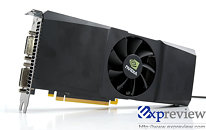
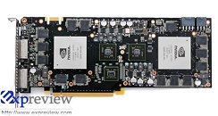
So it is true! NVIDIA does have a single-PCB GeForce GTX 295 accelerator in the works, and partners already seem to have access to it. The card must have had some serious development put into it, given the sheer complexity of the PCB (to cram two G200b GPUs, their display processors, and the PCI-E bridge chip, along with 28 memory chips). The accelerator first surfaced in the form of CAD drawings, in March.
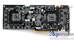
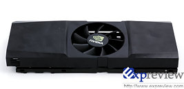
The PCB is pretty straight-forward: populate all the important logic on its business-side, and the memory on either sides. The card maintains its requirement for 8 + 6 pin PCI-E power input. Its VRM is spread across two main areas, to power a GPU system each. Internal SLI connects the two systems, while also providing support for Quad-SLI. Each GPU features 240 shader processors, along with 896 MB of GDDR3 memory across a 448-bit memory interface. Also pictured is the cooler: A fan nucleates the cooler, and blows in two opposite directions. The air is guided by the shroud onto two dense aluminum fin arrays that cool each GPU-system. The back of the card may use a heatspreader to cool the memory, like how the GeForce GTX 280 does it. While we don't expect this design to bring down the retail price of the card, we do believe that the design is mainly to provide partners, and retailers with decent margins that make selling the card a worthwhile venture. With the older design, it might not have been the case.

View at TechPowerUp Main Site
The PCB is pretty straight-forward: populate all the important logic on its business-side, and the memory on either sides. The card maintains its requirement for 8 + 6 pin PCI-E power input. Its VRM is spread across two main areas, to power a GPU system each. Internal SLI connects the two systems, while also providing support for Quad-SLI. Each GPU features 240 shader processors, along with 896 MB of GDDR3 memory across a 448-bit memory interface. Also pictured is the cooler: A fan nucleates the cooler, and blows in two opposite directions. The air is guided by the shroud onto two dense aluminum fin arrays that cool each GPU-system. The back of the card may use a heatspreader to cool the memory, like how the GeForce GTX 280 does it. While we don't expect this design to bring down the retail price of the card, we do believe that the design is mainly to provide partners, and retailers with decent margins that make selling the card a worthwhile venture. With the older design, it might not have been the case.


View at TechPowerUp Main Site
Last edited:


