- Joined
- Oct 9, 2007
- Messages
- 47,407 (7.51/day)
- Location
- Hyderabad, India
| System Name | RBMK-1000 |
|---|---|
| Processor | AMD Ryzen 7 5700G |
| Motherboard | ASUS ROG Strix B450-E Gaming |
| Cooling | DeepCool Gammax L240 V2 |
| Memory | 2x 8GB G.Skill Sniper X |
| Video Card(s) | Palit GeForce RTX 2080 SUPER GameRock |
| Storage | Western Digital Black NVMe 512GB |
| Display(s) | BenQ 1440p 60 Hz 27-inch |
| Case | Corsair Carbide 100R |
| Audio Device(s) | ASUS SupremeFX S1220A |
| Power Supply | Cooler Master MWE Gold 650W |
| Mouse | ASUS ROG Strix Impact |
| Keyboard | Gamdias Hermes E2 |
| Software | Windows 11 Pro |
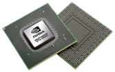
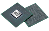
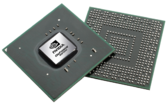
NVIDIA today announced its latest line of mobile graphics processors (mGPUs) based on the new 40 nm manufacturing technology. The GPUs also come as a surprise, as they embrace two technologies very few expected them to, this early/late. The GPUs support the DirectX 10.1 API, and some feature the new GDDR5 memory interface that doubles effective bandwidth. Enter GeForce GTS 260M, GTS 250M, GT 240M, GT 230M, and G 210M.
The G 210M succeeds the GeForce 9400, at least as far as the manufacturing technology and clock speeds go. It holds 16 shader processors, a 64-bit GDDR3 memory interface, and 512 MB of memory. The GT 230/240M hold 48 shaders, 1 GB of 128-bit GDDR3 memory, and clock-speeds that make up each variant. The GTS 260/250M are especially new, as they feature a 128-bit GDDR5 memory interface. 96 shaders and 1 GB of memory make the rest of their specs., while their clock speeds make for the variants. The table below spreads out the specifications.
The peculiar thing about these GPUs is their timing of entry into the market. This is the fag-end of the DirectX 10(.1) generation of GPUs, with no more high-end GPUs in sight. The company is facing stiff competition from AMD, and needs to cut manufacturing costs, while also decorating specs sheets. The use of GDDR5 allows manufacturers to narrow memory bus width, and reduce the number of memory chips, in turn board footprint, while maintaining the same levels of performance as GDDR3 with higher bus width. The use of 40 nm manufacturing process is certainly a step in the right direction, although we wonder how the company is able to get large yields of these chips, considering AMD isn't able to keep up with demand for its 40 nm GPUs, and is developing alternative SKUs at the same price points.
<table border="1" class="resulttable" cellspacing="0" cellpadding="3">
<tr>
<th></th>
<td>GeForce<br />
G 210M</td>
<td>GeForce<br />
GT 230M</td>
<td>GeForce <br />
GT 240M</td>
<td>GeForce<br>
GTS 250M</td>
<td>GeForce <br />
GTS 260M</td>
</tr>
<tr>
<th>Shader Units</th>
<td align="center">16</td>
<td align="center">48</td>
<td align="center">48</td>
<td align="center">96</td>
<td align="center">96</td>
</tr>
<tr>
<th>Memory Size</th>
<td align="center">512 MB</td>
<td align="center">1024 MB</td>
<td align="center">1024 MB</td>
<td align="center">1024 MB</td>
<td align="center">1024 MB</td>
</tr>
<tr>
<th>Memory Bus Width/Type </th>
<td align="center">64 bit GDDR3 </td>
<td align="center">128 bit GDDR3</td>
<td align="center">128 bit GDDR3</td>
<td align="center">128 bit GDDR5</td>
<td align="center">128 bit GDDR5</td>
<tr>
<th>Core/Shader/Memory Clock</th>
<td align="right">625/1500/800 MHz </td>
<td align="right">500/1100/800 MHz </td>
<td align="right">550/1210/800 MHz </td>
<td align="right">500/1250/800 (3.2 GT/s) MHz </td>
<td align="right">550/1375/900 (3.6 GT/s) MHz </td>
</table>
These GPUs will only be available to the mobile GPU board segment to begin with. There is no indication as to when the company makes desktop graphics cards based on these. AMD launched the RV740 in a similar fashion, with a mGPU board being released weeks ahead of the desktop board (Radeon HD 4770).
View at TechPowerUp Main Site
The G 210M succeeds the GeForce 9400, at least as far as the manufacturing technology and clock speeds go. It holds 16 shader processors, a 64-bit GDDR3 memory interface, and 512 MB of memory. The GT 230/240M hold 48 shaders, 1 GB of 128-bit GDDR3 memory, and clock-speeds that make up each variant. The GTS 260/250M are especially new, as they feature a 128-bit GDDR5 memory interface. 96 shaders and 1 GB of memory make the rest of their specs., while their clock speeds make for the variants. The table below spreads out the specifications.


The peculiar thing about these GPUs is their timing of entry into the market. This is the fag-end of the DirectX 10(.1) generation of GPUs, with no more high-end GPUs in sight. The company is facing stiff competition from AMD, and needs to cut manufacturing costs, while also decorating specs sheets. The use of GDDR5 allows manufacturers to narrow memory bus width, and reduce the number of memory chips, in turn board footprint, while maintaining the same levels of performance as GDDR3 with higher bus width. The use of 40 nm manufacturing process is certainly a step in the right direction, although we wonder how the company is able to get large yields of these chips, considering AMD isn't able to keep up with demand for its 40 nm GPUs, and is developing alternative SKUs at the same price points.
<table border="1" class="resulttable" cellspacing="0" cellpadding="3">
<tr>
<th></th>
<td>GeForce<br />
G 210M</td>
<td>GeForce<br />
GT 230M</td>
<td>GeForce <br />
GT 240M</td>
<td>GeForce<br>
GTS 250M</td>
<td>GeForce <br />
GTS 260M</td>
</tr>
<tr>
<th>Shader Units</th>
<td align="center">16</td>
<td align="center">48</td>
<td align="center">48</td>
<td align="center">96</td>
<td align="center">96</td>
</tr>
<tr>
<th>Memory Size</th>
<td align="center">512 MB</td>
<td align="center">1024 MB</td>
<td align="center">1024 MB</td>
<td align="center">1024 MB</td>
<td align="center">1024 MB</td>
</tr>
<tr>
<th>Memory Bus Width/Type </th>
<td align="center">64 bit GDDR3 </td>
<td align="center">128 bit GDDR3</td>
<td align="center">128 bit GDDR3</td>
<td align="center">128 bit GDDR5</td>
<td align="center">128 bit GDDR5</td>
<tr>
<th>Core/Shader/Memory Clock</th>
<td align="right">625/1500/800 MHz </td>
<td align="right">500/1100/800 MHz </td>
<td align="right">550/1210/800 MHz </td>
<td align="right">500/1250/800 (3.2 GT/s) MHz </td>
<td align="right">550/1375/900 (3.6 GT/s) MHz </td>
</table>
These GPUs will only be available to the mobile GPU board segment to begin with. There is no indication as to when the company makes desktop graphics cards based on these. AMD launched the RV740 in a similar fashion, with a mGPU board being released weeks ahead of the desktop board (Radeon HD 4770).
View at TechPowerUp Main Site
Last edited:


 These are pretty much just 8800GT's, any HD 4800 can beat that.
 . Seems quite crap, wish I could get 4870's in my lappy than a 9800GTX+.