- Joined
- Oct 9, 2007
- Messages
- 47,527 (7.48/day)
- Location
- Hyderabad, India
| System Name | RBMK-1000 |
|---|---|
| Processor | AMD Ryzen 7 5700G |
| Motherboard | ASUS ROG Strix B450-E Gaming |
| Cooling | DeepCool Gammax L240 V2 |
| Memory | 2x 8GB G.Skill Sniper X |
| Video Card(s) | Palit GeForce RTX 2080 SUPER GameRock |
| Storage | Western Digital Black NVMe 512GB |
| Display(s) | BenQ 1440p 60 Hz 27-inch |
| Case | Corsair Carbide 100R |
| Audio Device(s) | ASUS SupremeFX S1220A |
| Power Supply | Cooler Master MWE Gold 650W |
| Mouse | ASUS ROG Strix Impact |
| Keyboard | Gamdias Hermes E2 |
| Software | Windows 11 Pro |
Intel is on a golden path, showing no signs of a slowdown as far as technology development is concerned. After having pushed its 32 nm manufacturing node and its derived Westmere architecture to production grade, Intel seems to have already made a prototype on the 32 nm node, which will serve a technology leap on 32 nm. The company uses a "tick-tock" model of process development, where each processor architecture gets to be made in two manufacturing processes, while each process gets to build two succeeding architectures. The current Nehalem architecture meets 32 nm with the Westmere architecture, while the 32 nm node meets its next architecture with the SandyBridge.
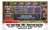
SandyBridge is characterised by a larger level of integration of components. While Nehalem and Westmere "Lynnfield" and "Clarksfield" mainstream processors use a multi-chip module that holds the CPU and north-bridge dice, SandyBridge will see an integration of both into a monolithic, rectangular die spreading across an area of around 225 sq. mm. Significant portions of the die will be occupied with a DirectX 11-compliant integrated graphics processor, the "SandyBridge System Agent" (a component which includes a PCI-Express hub, and DMI. The L3 cache is the largest component on the die. It will have a large 256-bit ring-topology, which lets it not only perform cache operations, but also as a fast transport medium between the various components.
There are four x86-64 processing cores with their own 256 KB L2 caches, and will feature the Advanced Vector eXtensions (AVX), the next generation SIMD instruction set. With so much packed, the chip will have a rated TDP of "only" 85W. When in production, it could come with clock speeds as high as 3.80 GHz. There is an indication that this chip will retain the LGA-1156 package to keep the upgrade path in progress. Interestingly, the chip is taped out in this quarter, while it will reach production-grade in the first quarter of 2011. Meanwhile LGA-1366 gets its next big thing with the Westmere-based Core i9 hexa-core processor.

View at TechPowerUp Main Site
SandyBridge is characterised by a larger level of integration of components. While Nehalem and Westmere "Lynnfield" and "Clarksfield" mainstream processors use a multi-chip module that holds the CPU and north-bridge dice, SandyBridge will see an integration of both into a monolithic, rectangular die spreading across an area of around 225 sq. mm. Significant portions of the die will be occupied with a DirectX 11-compliant integrated graphics processor, the "SandyBridge System Agent" (a component which includes a PCI-Express hub, and DMI. The L3 cache is the largest component on the die. It will have a large 256-bit ring-topology, which lets it not only perform cache operations, but also as a fast transport medium between the various components.
There are four x86-64 processing cores with their own 256 KB L2 caches, and will feature the Advanced Vector eXtensions (AVX), the next generation SIMD instruction set. With so much packed, the chip will have a rated TDP of "only" 85W. When in production, it could come with clock speeds as high as 3.80 GHz. There is an indication that this chip will retain the LGA-1156 package to keep the upgrade path in progress. Interestingly, the chip is taped out in this quarter, while it will reach production-grade in the first quarter of 2011. Meanwhile LGA-1366 gets its next big thing with the Westmere-based Core i9 hexa-core processor.

View at TechPowerUp Main Site
Last edited:


 Then we have 32kb L1 cache which is pretty standard and the 256kb present on core i7 and the 8mb L3 to make up for the lack of L2 cache but I don't think it will be enough compensation since the IGP is connected as well.