- Joined
- Oct 9, 2007
- Messages
- 47,435 (7.51/day)
- Location
- Hyderabad, India
| System Name | RBMK-1000 |
|---|---|
| Processor | AMD Ryzen 7 5700G |
| Motherboard | ASUS ROG Strix B450-E Gaming |
| Cooling | DeepCool Gammax L240 V2 |
| Memory | 2x 8GB G.Skill Sniper X |
| Video Card(s) | Palit GeForce RTX 2080 SUPER GameRock |
| Storage | Western Digital Black NVMe 512GB |
| Display(s) | BenQ 1440p 60 Hz 27-inch |
| Case | Corsair Carbide 100R |
| Audio Device(s) | ASUS SupremeFX S1220A |
| Power Supply | Cooler Master MWE Gold 650W |
| Mouse | ASUS ROG Strix Impact |
| Keyboard | Gamdias Hermes E2 |
| Software | Windows 11 Pro |
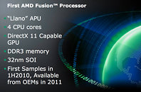
AMD, in its presentation at the International Solid State Circuits Conference (ISSCC) 2010, presented its plan to build its much talked about 'Fusion' processor platform, codenamed Llano, central to which, is the Accelerated Processing Unit (APU). AMD's APU is expected to be the first design to embed a multi-core x86 CPU and a GPU onto a single die. This design goes a notch ahead of Intel's recently released 'Clarkdale' processor, where Intel strapped a 32 nm dual-core CPU die and a 45 nm northbridge die with integrated graphics, onto an MCM (multi chip module) package. Llano is also expected to feature four processing cores, along with other design innovations.
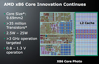
Some of the most notable announcements in AMD's presentation is that the company will begin sampling the chip to its industry partners within the first half of 2010. The Llano die will be build on a 32 nm High-K Metal Gate process. On this process, each x86 core will be as small as 9.69 mm². Other important components on the Llano die are a DDR3 memory controller, on-die northbridge, and a DirectX 11 compliant graphics core derived from the Evergreen family of GPUs. The x86 cores are expected to run at speeds of over 3 GHz. Each core has 1 MB of dedicated L2 cache, taking the total chip cache size to 4 MB.


AMD has also embraced some new power management technologies, including power gating. Power gating is a feature that allows the system to power down some x86 core to push their power draw to near-zero. This reduces the chip's overall power draw better, which also allows active cores to be powered up. Similar to Intel's Turbo Boost technology. The power aware clock grid design reduces power consumption by cutting down on clock distribution across the chip.
With the APU, AMD thinks it has the right product for tomorrow's market, a chip which packs a large chunk of the motherboard's silicon, while not compromising on the features due to space constraints within the package. There's room made for four processing cores, and an Evergreen-derived DirectX 11 compliant GPU. If implemented well enough on the software side, AMD believes it can deliver one chip that handles both serial processing workloads (by the x86 cores), and highly parallel workloads (by the stream processors). Market availability of the chip isn't definitively known, but we expect it to be out early next year, or late this year.
View at TechPowerUp Main Site
Some of the most notable announcements in AMD's presentation is that the company will begin sampling the chip to its industry partners within the first half of 2010. The Llano die will be build on a 32 nm High-K Metal Gate process. On this process, each x86 core will be as small as 9.69 mm². Other important components on the Llano die are a DDR3 memory controller, on-die northbridge, and a DirectX 11 compliant graphics core derived from the Evergreen family of GPUs. The x86 cores are expected to run at speeds of over 3 GHz. Each core has 1 MB of dedicated L2 cache, taking the total chip cache size to 4 MB.


AMD has also embraced some new power management technologies, including power gating. Power gating is a feature that allows the system to power down some x86 core to push their power draw to near-zero. This reduces the chip's overall power draw better, which also allows active cores to be powered up. Similar to Intel's Turbo Boost technology. The power aware clock grid design reduces power consumption by cutting down on clock distribution across the chip.
With the APU, AMD thinks it has the right product for tomorrow's market, a chip which packs a large chunk of the motherboard's silicon, while not compromising on the features due to space constraints within the package. There's room made for four processing cores, and an Evergreen-derived DirectX 11 compliant GPU. If implemented well enough on the software side, AMD believes it can deliver one chip that handles both serial processing workloads (by the x86 cores), and highly parallel workloads (by the stream processors). Market availability of the chip isn't definitively known, but we expect it to be out early next year, or late this year.
View at TechPowerUp Main Site


