- Joined
- Oct 9, 2007
- Messages
- 47,617 (7.44/day)
- Location
- Dublin, Ireland
| System Name | RBMK-1000 |
|---|---|
| Processor | AMD Ryzen 7 5700G |
| Motherboard | Gigabyte B550 AORUS Elite V2 |
| Cooling | DeepCool Gammax L240 V2 |
| Memory | 2x 16GB DDR4-3200 |
| Video Card(s) | Galax RTX 4070 Ti EX |
| Storage | Samsung 990 1TB |
| Display(s) | BenQ 1440p 60 Hz 27-inch |
| Case | Corsair Carbide 100R |
| Audio Device(s) | ASUS SupremeFX S1220A |
| Power Supply | Cooler Master MWE Gold 650W |
| Mouse | ASUS ROG Strix Impact |
| Keyboard | Gamdias Hermes E2 |
| Software | Windows 11 Pro |
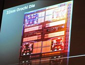
The first official die-shots of the first Bulldozer architecture derivative, the eight-core "Orochi" Opteron die was displayed at Global Technology Conference, by GlobalFoundries, AMD's principal foundry-partner. While AMD did not give out a die-map to go with it, the structures we can make out are four Bulldozer modules holding two cores and a shared L2 cache each, a L3 cache spread across four blocks that's shared between all cores, the northbridge-portion cutting across the die at the center, and the integrated memory controller along its far-right side. Various I/O portions are located along the other three sides.
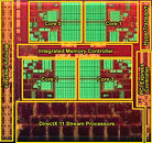
Next up is the Llano die. This is AMD's very first Fusion APU (accelerated processing unit) die. It is based on the K10 architecture and integrates a graphics processor and northbridge completely into one die. It precedes APUs based on the Bobcat architecture. Fortunately, there is a die-map at hand, which shows four K10 cores with dedicated 1 MB L2 caches per core, no L3 cache, an integrated SIMD array that holds 480 stream processors. The GPU component is DirectX 11 compliant. Other components include an integrated northbridge, integrated memory controller, integrated PCI-Express root complex, and HyperTransport interface to the chipset.


While Orochi is being built on 32 nm process, Llano is built on the 40 nm bulk process. AMD is designing the Orochi to compete with Intel's Sandy Bridge derived parts, while with the Llano Fusion APU, AMD is hoping to alter the casual gaming market dramatically. The APU's graphics processing capabilities are currently being measured to be on par with the ATI Radeon HD 5670 discrete GPU, while the quad-core CPU portion is built for the latest applications and games. AMD will pitch the Fusion APU as a one-piece solution that will offer both a fast processor, and GPU for performance home PCs, and casual gaming PCs.
View at TechPowerUp Main Site
Next up is the Llano die. This is AMD's very first Fusion APU (accelerated processing unit) die. It is based on the K10 architecture and integrates a graphics processor and northbridge completely into one die. It precedes APUs based on the Bobcat architecture. Fortunately, there is a die-map at hand, which shows four K10 cores with dedicated 1 MB L2 caches per core, no L3 cache, an integrated SIMD array that holds 480 stream processors. The GPU component is DirectX 11 compliant. Other components include an integrated northbridge, integrated memory controller, integrated PCI-Express root complex, and HyperTransport interface to the chipset.


While Orochi is being built on 32 nm process, Llano is built on the 40 nm bulk process. AMD is designing the Orochi to compete with Intel's Sandy Bridge derived parts, while with the Llano Fusion APU, AMD is hoping to alter the casual gaming market dramatically. The APU's graphics processing capabilities are currently being measured to be on par with the ATI Radeon HD 5670 discrete GPU, while the quad-core CPU portion is built for the latest applications and games. AMD will pitch the Fusion APU as a one-piece solution that will offer both a fast processor, and GPU for performance home PCs, and casual gaming PCs.
View at TechPowerUp Main Site
Last edited:


