- Joined
- Oct 9, 2007
- Messages
- 47,598 (7.45/day)
- Location
- Dublin, Ireland
| System Name | RBMK-1000 |
|---|---|
| Processor | AMD Ryzen 7 5700G |
| Motherboard | Gigabyte B550 AORUS Elite V2 |
| Cooling | DeepCool Gammax L240 V2 |
| Memory | 2x 16GB DDR4-3200 |
| Video Card(s) | Galax RTX 4070 Ti EX |
| Storage | Samsung 990 1TB |
| Display(s) | BenQ 1440p 60 Hz 27-inch |
| Case | Corsair Carbide 100R |
| Audio Device(s) | ASUS SupremeFX S1220A |
| Power Supply | Cooler Master MWE Gold 650W |
| Mouse | ASUS ROG Strix Impact |
| Keyboard | Gamdias Hermes E2 |
| Software | Windows 11 Pro |
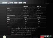
Barely a week after pictures of AMD's "Barts" prototype surfaced, it wasn't long before a specifications sheet followed. The all-important slide from AMD's presentation to its add-in board partners made it to sections of the Chinese media. "Barts" is a successor to "Juniper", on which are based the Radeon HD 5750 and HD 5770. The specs sheet reveals that while indeed the GPU looks to be larger physically, there are other factors that make it big:
Memory Controller
Barts has a 256-bit wide memory interface, which significantly increases its pin-count, and package-size. The "Pro" and "XT" variants (which will go on to be HD 6x50 and HD 6x70, respectively), have memory clocked at 1000 MHz and 1200 MHz, respectively, so that's nearly 100% increase in memory bandwidth .
Tiny increase in SIMD count, but major restructuring
Compared to Juniper, there seems to be an increase of only 20% in stream processor count physically. The XT variant has 960 stream processors, while the Pro variant has 800. AMD specifically mentioned SIMD block count, (10 enabled for Pro, 12 enabled for XT). If you noticed the slide, it says that the GPU is based on the "Cypress Dual Engine architecture", meaning that these 10 and 12 SIMD units will be spread across two blocks of 5 (Pro) or 6 (XT) SIMDs each, just like Cypress had two blocks of 10 SIMDs each.
Other components
The Raster Operations unit (ROP) count has been doubled to 32, TMUs stand at 40 for the Pro and 48 for the XT.
The design methodology is extremely simple. Juniper-based graphics cards anyway carry 8 memory chips to meet up to memory amount requirements of 1 GB using market-popular 1 Gbit GDDR5 chips, so why not just place those 8 chips across a 256-bit wide memory interface and double the memory bandwidth. The increased ROP count, coupled with up to 20% increase in shader compute power gives Barts the competitive edge it needs to face NVIDIA's reinvigorated GeForce 400 series after the introduction of the GeForce GTX 460. As for power draw, AMD projects the Pro variant to draw less than 150W, with the XT drawing "over" 150W.
Market Positioning
AMD doesn't have huge expectations from this. It has its task cut out: to compete with the GeForce GTX 460 768 MB and 1 GB models. While memory count ROP made the cut out NVIDIA's variants, AMD's come from clock speeds and SIMD core counts. It should then become obvious what these GPUs' pricing should look like.
When?
Usually when AMD gives out such a presentation to its AIB partners, a market release is about 3 months away.

View at TechPowerUp Main Site
Memory Controller
Barts has a 256-bit wide memory interface, which significantly increases its pin-count, and package-size. The "Pro" and "XT" variants (which will go on to be HD 6x50 and HD 6x70, respectively), have memory clocked at 1000 MHz and 1200 MHz, respectively, so that's nearly 100% increase in memory bandwidth .
Tiny increase in SIMD count, but major restructuring
Compared to Juniper, there seems to be an increase of only 20% in stream processor count physically. The XT variant has 960 stream processors, while the Pro variant has 800. AMD specifically mentioned SIMD block count, (10 enabled for Pro, 12 enabled for XT). If you noticed the slide, it says that the GPU is based on the "Cypress Dual Engine architecture", meaning that these 10 and 12 SIMD units will be spread across two blocks of 5 (Pro) or 6 (XT) SIMDs each, just like Cypress had two blocks of 10 SIMDs each.
Other components
The Raster Operations unit (ROP) count has been doubled to 32, TMUs stand at 40 for the Pro and 48 for the XT.
The design methodology is extremely simple. Juniper-based graphics cards anyway carry 8 memory chips to meet up to memory amount requirements of 1 GB using market-popular 1 Gbit GDDR5 chips, so why not just place those 8 chips across a 256-bit wide memory interface and double the memory bandwidth. The increased ROP count, coupled with up to 20% increase in shader compute power gives Barts the competitive edge it needs to face NVIDIA's reinvigorated GeForce 400 series after the introduction of the GeForce GTX 460. As for power draw, AMD projects the Pro variant to draw less than 150W, with the XT drawing "over" 150W.
Market Positioning
AMD doesn't have huge expectations from this. It has its task cut out: to compete with the GeForce GTX 460 768 MB and 1 GB models. While memory count ROP made the cut out NVIDIA's variants, AMD's come from clock speeds and SIMD core counts. It should then become obvious what these GPUs' pricing should look like.
When?
Usually when AMD gives out such a presentation to its AIB partners, a market release is about 3 months away.

View at TechPowerUp Main Site
Last edited:


 , but hearing all the rumours about the HD6770 is going to be name the HD6870

