- Joined
- Oct 9, 2007
- Messages
- 47,604 (7.45/day)
- Location
- Dublin, Ireland
| System Name | RBMK-1000 |
|---|---|
| Processor | AMD Ryzen 7 5700G |
| Motherboard | Gigabyte B550 AORUS Elite V2 |
| Cooling | DeepCool Gammax L240 V2 |
| Memory | 2x 16GB DDR4-3200 |
| Video Card(s) | Galax RTX 4070 Ti EX |
| Storage | Samsung 990 1TB |
| Display(s) | BenQ 1440p 60 Hz 27-inch |
| Case | Corsair Carbide 100R |
| Audio Device(s) | ASUS SupremeFX S1220A |
| Power Supply | Cooler Master MWE Gold 650W |
| Mouse | ASUS ROG Strix Impact |
| Keyboard | Gamdias Hermes E2 |
| Software | Windows 11 Pro |
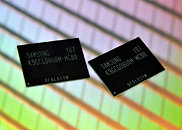
Samsung Electronics Co., Ltd., the world leader in advanced memory technology, today announced that it has started the industry's first production of a high-performance toggle DDR 2.0 multi-level-cell (MLC) memory chip. The new NAND flash chip features a 64 gigabit (Gb) density, made possible by using an advanced 20 nanometer (nm) class* process technology. The chip is designed to support the high-performance requirements of mobile devices such as smartphones, tablets and solid state drives (SSDs).
Equipped with a toggle DDR (Double Data Rate) 2.0 interface, the new 64Gb MLC chip can transmit data at a bandwidth of up to 400 megabit per second (Mbps). This provides a 10-fold increase over the 40Mbps Single Data Rate (SDR) NAND flash memory in widespread use today, and a three-fold boost over 133Mbps toggle DDR 1.0, 32Gb NAND flash memory, which Samsung was first to produce in 2009.

"With this 20nm-class, 64Gb, toggle DDR 2.0 NAND, Samsung is leading the market, which is evolving to fourth-generation smartphones and SATA 6Gbps SSDs," said Wanhoon Hong, executive vice president, memory sales & marketing, Samsung Electronics. "We will continue to aggressively develop the world's most advanced toggle DDR NAND flash solutions with higher performance and density, since we see them as vital to enabling a greater diversity of services for mobile phone users worldwide."
The high-speed 400Mbps bandwidth of toggle DDR 2.0 is expected to better support the ongoing shift toward advanced interfaces, as more mobile and consumer electronics devices requiring added performance and higher densities adopt new interfaces such as USB 3.0 and SATA 6.0Gbps,
Further, the new 64Gb MLC NAND chip offers an approximate 50-percent increase in productivity over 20nm-class 32Gb MLC NAND chips with a toggle DDR 1.0 interface (which Samsung started producing in April last year) and more than doubles the productivity of 30nm-class 32Gb MLC NAND.
According to IHS iSuppli, the worldwide NAND flash memory market will continue to steadily grow from approximately 11 billion 1 Gigabyte (GB) equivalent unitsin 2010 to 94 billion 1GB equivalent units in 2015 with a CAGR of 54 percent. In addition, shipments of NAND flash memory with 64Gb or higher density are expected to account for approximately 70 percent of total NAND flash memory shipments in 2012, a huge increase from the three percent level in 2010.
* 20 nm class = 20~29 nm
View at TechPowerUp Main Site
Equipped with a toggle DDR (Double Data Rate) 2.0 interface, the new 64Gb MLC chip can transmit data at a bandwidth of up to 400 megabit per second (Mbps). This provides a 10-fold increase over the 40Mbps Single Data Rate (SDR) NAND flash memory in widespread use today, and a three-fold boost over 133Mbps toggle DDR 1.0, 32Gb NAND flash memory, which Samsung was first to produce in 2009.

"With this 20nm-class, 64Gb, toggle DDR 2.0 NAND, Samsung is leading the market, which is evolving to fourth-generation smartphones and SATA 6Gbps SSDs," said Wanhoon Hong, executive vice president, memory sales & marketing, Samsung Electronics. "We will continue to aggressively develop the world's most advanced toggle DDR NAND flash solutions with higher performance and density, since we see them as vital to enabling a greater diversity of services for mobile phone users worldwide."
The high-speed 400Mbps bandwidth of toggle DDR 2.0 is expected to better support the ongoing shift toward advanced interfaces, as more mobile and consumer electronics devices requiring added performance and higher densities adopt new interfaces such as USB 3.0 and SATA 6.0Gbps,
Further, the new 64Gb MLC NAND chip offers an approximate 50-percent increase in productivity over 20nm-class 32Gb MLC NAND chips with a toggle DDR 1.0 interface (which Samsung started producing in April last year) and more than doubles the productivity of 30nm-class 32Gb MLC NAND.
According to IHS iSuppli, the worldwide NAND flash memory market will continue to steadily grow from approximately 11 billion 1 Gigabyte (GB) equivalent unitsin 2010 to 94 billion 1GB equivalent units in 2015 with a CAGR of 54 percent. In addition, shipments of NAND flash memory with 64Gb or higher density are expected to account for approximately 70 percent of total NAND flash memory shipments in 2012, a huge increase from the three percent level in 2010.
* 20 nm class = 20~29 nm
View at TechPowerUp Main Site


