- Joined
- Oct 9, 2007
- Messages
- 47,655 (7.43/day)
- Location
- Dublin, Ireland
| System Name | RBMK-1000 |
|---|---|
| Processor | AMD Ryzen 7 5700G |
| Motherboard | Gigabyte B550 AORUS Elite V2 |
| Cooling | DeepCool Gammax L240 V2 |
| Memory | 2x 16GB DDR4-3200 |
| Video Card(s) | Galax RTX 4070 Ti EX |
| Storage | Samsung 990 1TB |
| Display(s) | BenQ 1440p 60 Hz 27-inch |
| Case | Corsair Carbide 100R |
| Audio Device(s) | ASUS SupremeFX S1220A |
| Power Supply | Cooler Master MWE Gold 650W |
| Mouse | ASUS ROG Strix Impact |
| Keyboard | Gamdias Hermes E2 |
| Software | Windows 11 Pro |
Intel is making serious efforts to boost CPU-integrated graphics performance using homegrown architectures, without having to borrow/license any technologies from the other two major players in the PC graphics business that have technological edges over Intel, and hence make high-performance discrete-GPUs (NVIDIA and AMD). Intel's architecture that succeeds Ivy Bridge, codenamed Haswell, will be at the receiving-end of a significant advancement in GPU performance.
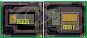
We know from history, that Intel carves out variants of chips using a common silicon, by toggling the amount of L3 cache available, number of cores, and even number of iGPU shaders, apart from other natural handles such as clock speeds, voltages, and feature-set. With Haswell, the highest iGPU configuration will make use of a 4th-level cache (L4 cache), that sits on the package, while not being a part of the Haswell silicon. The Haswell silicon will instead be placed on a multi-chip module (MCM) along with a separate die that holds this L4 cache. The L4 cache will serve as a fast memory for the iGPU, while reducing or completely offloading the iGPU's dependency on the system memory as a frame-buffer (UMA).

Such implementations aren't entirely new. IBM has used what's known as the eDRAM (embedded-DRAM), a separate silicon with fast memory and some low-level graphics logic, on some of its its game console processor ASICs. AMD, too, used a technology that's similar in principle, though not in implementation. Certain higher-end 7-series and 8-series graphics chipsets (such as AMD 780G, 790GX, and 890GX) feature what's known as DDR3-Sideport memory, which gives the Radeon IGP access to about 128 MB of fast DDR3 memory, which it can use standalone to offload system memory (UMA), or interleave with it (UMA+Sideport).
Could this be the what Intel is referring to as "Hotham 1.0"?
View at TechPowerUp Main Site
We know from history, that Intel carves out variants of chips using a common silicon, by toggling the amount of L3 cache available, number of cores, and even number of iGPU shaders, apart from other natural handles such as clock speeds, voltages, and feature-set. With Haswell, the highest iGPU configuration will make use of a 4th-level cache (L4 cache), that sits on the package, while not being a part of the Haswell silicon. The Haswell silicon will instead be placed on a multi-chip module (MCM) along with a separate die that holds this L4 cache. The L4 cache will serve as a fast memory for the iGPU, while reducing or completely offloading the iGPU's dependency on the system memory as a frame-buffer (UMA).

Such implementations aren't entirely new. IBM has used what's known as the eDRAM (embedded-DRAM), a separate silicon with fast memory and some low-level graphics logic, on some of its its game console processor ASICs. AMD, too, used a technology that's similar in principle, though not in implementation. Certain higher-end 7-series and 8-series graphics chipsets (such as AMD 780G, 790GX, and 890GX) feature what's known as DDR3-Sideport memory, which gives the Radeon IGP access to about 128 MB of fast DDR3 memory, which it can use standalone to offload system memory (UMA), or interleave with it (UMA+Sideport).
Could this be the what Intel is referring to as "Hotham 1.0"?
View at TechPowerUp Main Site


