- Joined
- Oct 9, 2007
- Messages
- 47,538 (7.46/day)
- Location
- Hyderabad, India
| System Name | RBMK-1000 |
|---|---|
| Processor | AMD Ryzen 7 5700G |
| Motherboard | ASUS ROG Strix B450-E Gaming |
| Cooling | DeepCool Gammax L240 V2 |
| Memory | 2x 8GB G.Skill Sniper X |
| Video Card(s) | Palit GeForce RTX 2080 SUPER GameRock |
| Storage | Western Digital Black NVMe 512GB |
| Display(s) | BenQ 1440p 60 Hz 27-inch |
| Case | Corsair Carbide 100R |
| Audio Device(s) | ASUS SupremeFX S1220A |
| Power Supply | Cooler Master MWE Gold 650W |
| Mouse | ASUS ROG Strix Impact |
| Keyboard | Gamdias Hermes E2 |
| Software | Windows 11 Pro |
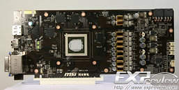
MSI's flagship factory-overclocked graphics card based on the GeForce GTX 660, the N660GTX HAWK, was pictured and detailed by Expreview, earlier this week. According to the source, the card will be designed for about 15% higher core clock speeds than reference, backed by high-grade voltage regulation circuitry and the company's TwinFrozr IV cooling solution.
To begin with, the GeForce GTX 660 HAWK will ship with clock speeds of 1100 MHz core, 1176 MHz GPU Boost core clock speeds. The memory is left untouched at 6.00 GHz (GDDR5-effective). Under the hood is a 10-phase VRM that uses SSC chokes (low energy loss to noise), and IR DirectFETs. The card appears to use a high-end voltage controller that allows software voltage control, and consolidated voltage measurement points. The card draws power from two 6-pin PCIe power connectors.


Another striking feature of the GTX 660 HAWK is dual-BIOS. The card packs two physical EEPROM chips that can be toggled with a small switch along the card's length. One of the two packs the factory-OC clock/voltage profile, while the other retains a fail-safe NVIDIA-reference clock speed profile. The card also features MSI's GPU Reactor module that adds an additional set of tantalum capacitors, and ensures cleaner voltage delivery to the GPU.
Based on the 28 nm GK106 silicon, the GeForce GTX 660 packs 960 CUDA cores, 80 TMUs, 24 ROPs, and a 192-bit wide GDDR5 memory interface, holding 2 GB of memory. Display outputs include two DVI, and one each of DisplayPort and HDMI. The card can pair with any other GTX 660 card for 2-way SLI. The source did not reveal availability information.
View at TechPowerUp Main Site
To begin with, the GeForce GTX 660 HAWK will ship with clock speeds of 1100 MHz core, 1176 MHz GPU Boost core clock speeds. The memory is left untouched at 6.00 GHz (GDDR5-effective). Under the hood is a 10-phase VRM that uses SSC chokes (low energy loss to noise), and IR DirectFETs. The card appears to use a high-end voltage controller that allows software voltage control, and consolidated voltage measurement points. The card draws power from two 6-pin PCIe power connectors.


Another striking feature of the GTX 660 HAWK is dual-BIOS. The card packs two physical EEPROM chips that can be toggled with a small switch along the card's length. One of the two packs the factory-OC clock/voltage profile, while the other retains a fail-safe NVIDIA-reference clock speed profile. The card also features MSI's GPU Reactor module that adds an additional set of tantalum capacitors, and ensures cleaner voltage delivery to the GPU.
Based on the 28 nm GK106 silicon, the GeForce GTX 660 packs 960 CUDA cores, 80 TMUs, 24 ROPs, and a 192-bit wide GDDR5 memory interface, holding 2 GB of memory. Display outputs include two DVI, and one each of DisplayPort and HDMI. The card can pair with any other GTX 660 card for 2-way SLI. The source did not reveal availability information.
View at TechPowerUp Main Site


