- Joined
- Oct 9, 2007
- Messages
- 47,853 (7.38/day)
- Location
- Dublin, Ireland
| System Name | RBMK-1000 |
|---|---|
| Processor | AMD Ryzen 7 5700G |
| Motherboard | Gigabyte B550 AORUS Elite V2 |
| Cooling | DeepCool Gammax L240 V2 |
| Memory | 2x 16GB DDR4-3200 |
| Video Card(s) | Galax RTX 4070 Ti EX |
| Storage | Samsung 990 1TB |
| Display(s) | BenQ 1440p 60 Hz 27-inch |
| Case | Corsair Carbide 100R |
| Audio Device(s) | ASUS SupremeFX S1220A |
| Power Supply | Cooler Master MWE Gold 650W |
| Mouse | ASUS ROG Strix Impact |
| Keyboard | Gamdias Hermes E2 |
| Software | Windows 11 Pro |
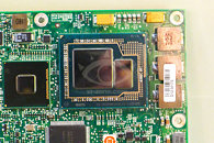
To tackle upcoming generations of Ultrabooks and NUC that lack space for discrete graphics, yet having to keep up with the demands of higher display resolutions (i.e. proliferation of 3840 x 2160), Intel is designing special variants of its Core "Haswell" processors that feature large integrated graphics cores bolstered by fourth-level eDRAM caches on-package. Pictured below, is one such contraption.
The graphics-enhanced Core "Haswell" processor is an MCM (multi-chip module) of two dies, the larger one is the actual "Haswell" processor complex with cores, uncore, and the larger GT3 integrated graphics core. While the standard Haswell silicon with GT1 and GT2 integrated GPU options, physically features up to 20 execution units (EUs), the large GT3 silicon features double that, at 40 EUs.
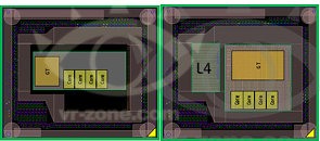
The first slide below details the Haswell GT3 package, while the second one details a standard Core "Haswell" implementation. You'll notice that apart from a larger graphics core, the processor features an additional stop on its ring-bus, the eDRAM PHY, interfacing with an external eDRAM silicon (the smaller chip on the MCM). Treated as L4 cache, the eDRAM chip provides higher bandwidth and lower latency than the main memory, for the graphics core to temporarily hold whatever it's working on, without clogging the main memory bus much. This is similar in principle to AMD's Sideport Memory, use of small amounts of faster memory on the motherboard to boost integrated graphics performance.
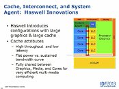
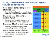
Haswell GT3 is being designed to offer graphics performance that rivals discrete GPUs from NVIDIA and AMD under the 20W TDP envelope. Haswell GT3 (the entire package) itself features a TDP of 55W, which may seem high for Ultrabooks, but are backed by power management features that work to reduce the net power draw. Intel believes Haswell GT3 could provide a viable alternative to standard Haswell silicon aided by discrete GPUs.
View at TechPowerUp Main Site
The graphics-enhanced Core "Haswell" processor is an MCM (multi-chip module) of two dies, the larger one is the actual "Haswell" processor complex with cores, uncore, and the larger GT3 integrated graphics core. While the standard Haswell silicon with GT1 and GT2 integrated GPU options, physically features up to 20 execution units (EUs), the large GT3 silicon features double that, at 40 EUs.


The first slide below details the Haswell GT3 package, while the second one details a standard Core "Haswell" implementation. You'll notice that apart from a larger graphics core, the processor features an additional stop on its ring-bus, the eDRAM PHY, interfacing with an external eDRAM silicon (the smaller chip on the MCM). Treated as L4 cache, the eDRAM chip provides higher bandwidth and lower latency than the main memory, for the graphics core to temporarily hold whatever it's working on, without clogging the main memory bus much. This is similar in principle to AMD's Sideport Memory, use of small amounts of faster memory on the motherboard to boost integrated graphics performance.


Haswell GT3 is being designed to offer graphics performance that rivals discrete GPUs from NVIDIA and AMD under the 20W TDP envelope. Haswell GT3 (the entire package) itself features a TDP of 55W, which may seem high for Ultrabooks, but are backed by power management features that work to reduce the net power draw. Intel believes Haswell GT3 could provide a viable alternative to standard Haswell silicon aided by discrete GPUs.
View at TechPowerUp Main Site
Last edited:


