- Joined
- Oct 9, 2007
- Messages
- 47,527 (7.48/day)
- Location
- Hyderabad, India
| System Name | RBMK-1000 |
|---|---|
| Processor | AMD Ryzen 7 5700G |
| Motherboard | ASUS ROG Strix B450-E Gaming |
| Cooling | DeepCool Gammax L240 V2 |
| Memory | 2x 8GB G.Skill Sniper X |
| Video Card(s) | Palit GeForce RTX 2080 SUPER GameRock |
| Storage | Western Digital Black NVMe 512GB |
| Display(s) | BenQ 1440p 60 Hz 27-inch |
| Case | Corsair Carbide 100R |
| Audio Device(s) | ASUS SupremeFX S1220A |
| Power Supply | Cooler Master MWE Gold 650W |
| Mouse | ASUS ROG Strix Impact |
| Keyboard | Gamdias Hermes E2 |
| Software | Windows 11 Pro |
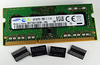
Samsung Electronics Co., Ltd., the world leader in memory technology, today announced that it is mass producing the most advanced DDR3 memory, based on a new 20 nanometer process technology, for use in a wide range of computing applications. Samsung has pushed the envelope of DRAM scaling, while utilizing currently available immersion ArF lithography, in its roll-out of the industry's most advanced 20-nanometer (nm) 4-gigabit (Gb) DDR3 DRAM.
With DRAM memory, where each cell consists of a capacitor and a transistor linked to one another, scaling is more difficult than with NAND Flash memory in which a cell only needs a transistor. To continue scaling for more advanced DRAM, Samsung refined its design and manufacturing technologies and came up with a modified double patterning and atomic layer deposition.

Samsung's modified double patterning technology marks a new milestone, by enabling 20nm DDR3 production using current photolithography equipment and establishing the core technology for the next generation of 10nm-class DRAM production. Samsung also successfully created ultrathin dielectric layers of cell capacitors with an unprecedented uniformity, which has resulted in higher cell performance.
With the new 20nm DDR3 DRAM applying these technologies, Samsung also has improved manufacturing productivity, which is over 30 percent higher than that of the preceding 25 nanometer DDR3, and more than twice that of 30nm-class* DDR3.
In addition, the new 20nm 4Gb DDR3- based modules can save up to 25 percent of the energy consumed by equivalent modules fabricated using the previous 25 nanometer process technology. This improvement provides the basis for delivering the industry's most advanced green IT solutions to global companies.
"Samsung's new energy-efficient 20-nanometer DDR3 DRAM will rapidly expand its market base throughout the IT industry including the PC and mobile markets, quickly moving to mainstream status," said Young-Hyun Jun, executive vice president, memory sales and marketing, Samsung Electronics. "Samsung will continue to deliver next-generation DRAM and green memory solutions ahead of the competition, while contributing to the growth of the global IT market in close cooperation with our major customers."
According to market research data from Gartner, the global DRAM market will grow from $35.6 billion US dollars in 2013 to $37.9 billion US dollars in 2014.
View at TechPowerUp Main Site
With DRAM memory, where each cell consists of a capacitor and a transistor linked to one another, scaling is more difficult than with NAND Flash memory in which a cell only needs a transistor. To continue scaling for more advanced DRAM, Samsung refined its design and manufacturing technologies and came up with a modified double patterning and atomic layer deposition.

Samsung's modified double patterning technology marks a new milestone, by enabling 20nm DDR3 production using current photolithography equipment and establishing the core technology for the next generation of 10nm-class DRAM production. Samsung also successfully created ultrathin dielectric layers of cell capacitors with an unprecedented uniformity, which has resulted in higher cell performance.
With the new 20nm DDR3 DRAM applying these technologies, Samsung also has improved manufacturing productivity, which is over 30 percent higher than that of the preceding 25 nanometer DDR3, and more than twice that of 30nm-class* DDR3.
In addition, the new 20nm 4Gb DDR3- based modules can save up to 25 percent of the energy consumed by equivalent modules fabricated using the previous 25 nanometer process technology. This improvement provides the basis for delivering the industry's most advanced green IT solutions to global companies.
"Samsung's new energy-efficient 20-nanometer DDR3 DRAM will rapidly expand its market base throughout the IT industry including the PC and mobile markets, quickly moving to mainstream status," said Young-Hyun Jun, executive vice president, memory sales and marketing, Samsung Electronics. "Samsung will continue to deliver next-generation DRAM and green memory solutions ahead of the competition, while contributing to the growth of the global IT market in close cooperation with our major customers."
According to market research data from Gartner, the global DRAM market will grow from $35.6 billion US dollars in 2013 to $37.9 billion US dollars in 2014.
View at TechPowerUp Main Site


