- Joined
- Oct 9, 2007
- Messages
- 47,619 (7.44/day)
- Location
- Dublin, Ireland
| System Name | RBMK-1000 |
|---|---|
| Processor | AMD Ryzen 7 5700G |
| Motherboard | Gigabyte B550 AORUS Elite V2 |
| Cooling | DeepCool Gammax L240 V2 |
| Memory | 2x 16GB DDR4-3200 |
| Video Card(s) | Galax RTX 4070 Ti EX |
| Storage | Samsung 990 1TB |
| Display(s) | BenQ 1440p 60 Hz 27-inch |
| Case | Corsair Carbide 100R |
| Audio Device(s) | ASUS SupremeFX S1220A |
| Power Supply | Cooler Master MWE Gold 650W |
| Mouse | ASUS ROG Strix Impact |
| Keyboard | Gamdias Hermes E2 |
| Software | Windows 11 Pro |
NVIDIA's "Maxwell" architecture may have got a rather low-key debut with the GeForce GTX 750 Ti, but nobody saw its performance-segment derivative, the GM204 silicon, driving the GeForce GTX 980 and the GTX 970. The new architecture makes its predecessor, the "Kepler" look inefficient in comparison. It looks like NVIDIA still thinks Kepler is competitive to competition from AMD (GCN) and Intel (Knights Corner), in the high-performance computing era.
The problems here are NVIDIA already launched a GK110 based Tesla HPC card, and its big "Maxwell" chip is nowhere in sight. The GM204 has limited memory bandwidth, and its texture-compression mojo can't bail out bandwidth-hogging HPC applications. The solution? Develop a new big silicon based on "Kepler." Enter, the GK210. That's right, the G-K-210. Launched today with the Tesla K80 dual-chip HPC accelerator, this chip could feature design improvements over the GK110, while offering memory bandwidth and sizes not possible on the GM204.

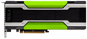
The Tesla K80 accelerator is a dual-chip solution, with two GK210 chips. Each of the two features 2,496 CUDA cores, totaling 4,992 in all. Each chip features a 384-bit wide GDDR5 memory interface, wired to 12 GB of memory. That gives the K80 a staggering 24 GB of memory, across two 240 GB/s memory interfaces. 240 GB/s may not seem like a figure a GM204 can't achieve, but we're beyond consumer (GeForce) and enterprise (Quadro) market-segments here, entering the mission-critical (Tesla) one. NVIDIA is clocking the card very conservatively. The Tesla isn't a graphics card to begin with. Its core runs at 562 MHz, which can spool up to 875 MHz, and the memory ticks at 5.00 GHz, less than the 6 GHz on the Tesla K40.
So what's changed between the GK210 and the GK110? For one, it appears to be extremely energy efficient. The Tesla K80 comes with passive cooling (relies on the air-flow of the rackmount blade it's part of), and has a TDP rating of 300W (150W per GPU system). In comparison, the single-chip Tesla K40 is rated at 235W. The Boost clocks of both chips are identical, even if the nominal clocks on the Tesla K80's GK210 are marginally lower, and the memory clocks lower by 15%. Another technical difference between the GK210 and the GK110 is under the hood.
While both chips are based on the "Kepler" architecture, GK210 features double the shader cache amount. Each of the 15 streaming multiprocessors (SMXs) features 128 KB of shader cache, compared to 64 KB per SMX on the GK110. The GK210 also has a 512 KB register file per SMX, double the size of the 256 KB register file size, of the GK110. A larger register file size means that the number of variables a shader can use is increased. If an operation runs out of register, then those variables have to sit in the chip's limited last-level cache, taking more clock cycles to fetch, or even worse, the GPU memory, which is several orders of magnitude slower. These two changes could step up the GPU's serial processing performance slightly, while retaining its inherent parallel processing advantages, which could really help in an HPC environment. In other words, we won't hold our breath for a consumer GeForce debut of this chip.
View at TechPowerUp Main Site
The problems here are NVIDIA already launched a GK110 based Tesla HPC card, and its big "Maxwell" chip is nowhere in sight. The GM204 has limited memory bandwidth, and its texture-compression mojo can't bail out bandwidth-hogging HPC applications. The solution? Develop a new big silicon based on "Kepler." Enter, the GK210. That's right, the G-K-210. Launched today with the Tesla K80 dual-chip HPC accelerator, this chip could feature design improvements over the GK110, while offering memory bandwidth and sizes not possible on the GM204.

The Tesla K80 accelerator is a dual-chip solution, with two GK210 chips. Each of the two features 2,496 CUDA cores, totaling 4,992 in all. Each chip features a 384-bit wide GDDR5 memory interface, wired to 12 GB of memory. That gives the K80 a staggering 24 GB of memory, across two 240 GB/s memory interfaces. 240 GB/s may not seem like a figure a GM204 can't achieve, but we're beyond consumer (GeForce) and enterprise (Quadro) market-segments here, entering the mission-critical (Tesla) one. NVIDIA is clocking the card very conservatively. The Tesla isn't a graphics card to begin with. Its core runs at 562 MHz, which can spool up to 875 MHz, and the memory ticks at 5.00 GHz, less than the 6 GHz on the Tesla K40.
So what's changed between the GK210 and the GK110? For one, it appears to be extremely energy efficient. The Tesla K80 comes with passive cooling (relies on the air-flow of the rackmount blade it's part of), and has a TDP rating of 300W (150W per GPU system). In comparison, the single-chip Tesla K40 is rated at 235W. The Boost clocks of both chips are identical, even if the nominal clocks on the Tesla K80's GK210 are marginally lower, and the memory clocks lower by 15%. Another technical difference between the GK210 and the GK110 is under the hood.
While both chips are based on the "Kepler" architecture, GK210 features double the shader cache amount. Each of the 15 streaming multiprocessors (SMXs) features 128 KB of shader cache, compared to 64 KB per SMX on the GK110. The GK210 also has a 512 KB register file per SMX, double the size of the 256 KB register file size, of the GK110. A larger register file size means that the number of variables a shader can use is increased. If an operation runs out of register, then those variables have to sit in the chip's limited last-level cache, taking more clock cycles to fetch, or even worse, the GPU memory, which is several orders of magnitude slower. These two changes could step up the GPU's serial processing performance slightly, while retaining its inherent parallel processing advantages, which could really help in an HPC environment. In other words, we won't hold our breath for a consumer GeForce debut of this chip.
View at TechPowerUp Main Site


