- Joined
- Oct 9, 2007
- Messages
- 47,647 (7.44/day)
- Location
- Dublin, Ireland
| System Name | RBMK-1000 |
|---|---|
| Processor | AMD Ryzen 7 5700G |
| Motherboard | Gigabyte B550 AORUS Elite V2 |
| Cooling | DeepCool Gammax L240 V2 |
| Memory | 2x 16GB DDR4-3200 |
| Video Card(s) | Galax RTX 4070 Ti EX |
| Storage | Samsung 990 1TB |
| Display(s) | BenQ 1440p 60 Hz 27-inch |
| Case | Corsair Carbide 100R |
| Audio Device(s) | ASUS SupremeFX S1220A |
| Power Supply | Cooler Master MWE Gold 650W |
| Mouse | ASUS ROG Strix Impact |
| Keyboard | Gamdias Hermes E2 |
| Software | Windows 11 Pro |
Some of the first CPUs and APUs based on AMD's next-generation "Zen" micro-architecture could be quad-core. "Zen" will be AMD's first monolithic core design after a stint with multi-core modules, with its "Bulldozer" architecture. Our older article details what sets Zen apart from its predecessor. As expected, in a multi-core chip, Zen cores share no hardware resources with each other, than a last-level cache (L3 cache), much like Intel's current CPU architecture.
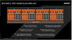
There's just one area where Zen will differ from Haswell. With Haswell, Intel has shown that it can clump any number of cores on a chip, and make them share a proportionately large L3 cache. Haswell-E features 8 cores sharing a 20 MB cache. The Haswell-EX features 18 cores sharing 45 MB of cache. With Zen, however, the scale up stops at 4 cores sharing 8 MB of L3 cache. A set of four cores makes up what AMD calls a "quad-core unit." To be absolutely clear, this is not a module, the cores share no hardware components with each other, besides the L3 cache.

For AMD to build chips with more than 4 cores, the company will have to scale up the number of such "quad-core units." A mainstream APU will likely feature just one unit, with four cores. A high-end desktop chip will likely feature two units, making up 8 cores, and 16 MB of total L3 cache, 8 MB shared between four cores, each. Bigger enterprise Opteron chips could take that count up to 4 units, making up 16 cores, and 32 MB of L3 cache. What also makes this "quad-core unit" different from a module is that it's divisible. You can, in theory, carve out dual-core parts using these units.
AMD's clumping four cores together appears to be a harvesting measure, much like Intel's Haswell silicon. Even a Core i3-4160 dual-core chip features a silicon with four physical cores, but two disabled. Which two get disabled depends on either random selection (if all four cores are perfect) or on which two cores are most functional. So a dual-core "Haswell" has a combination of any two of the cores physically present. The 8 MB of L3 cache on a Haswell silicon has ring-stops that allow SKU designers to let the CPU address 2 MB, 3 MB, 4 MB, 6 MB, or all 8 MB of it.
How AMD plans to package these chips, remains a mystery. We've heard too many reports eulogizing AM3+, and AMD's inefficient 3-chip platform design, which Intel junked way back in 2008, with its X58 HEDT platform. One could imagine AMD to come up with a new high-end desktop processor package, which lacks integrated graphics on its silicon, but crams in eight cores, 16 MB of cache, a dual-channel DDR4 IMC, and a 40-lane PCI-Express gen 3.0 root complex, if not 24-lane, like its APU counterparts. The current FM2+ socket looks ready for "Zen" based mainstream/performance APUs from a technical standpoint.
The key to "Zen" success, however, is AMD getting the energy-efficiency right, and for that, it's betting heavily on foundry-partner GlobalFoundries to get its 14 nanometer FinFET node up and running. This report from Expreview suggests that the company's Dresden-based facility is just about ready with its 14 nm node.
View at TechPowerUp Main Site
There's just one area where Zen will differ from Haswell. With Haswell, Intel has shown that it can clump any number of cores on a chip, and make them share a proportionately large L3 cache. Haswell-E features 8 cores sharing a 20 MB cache. The Haswell-EX features 18 cores sharing 45 MB of cache. With Zen, however, the scale up stops at 4 cores sharing 8 MB of L3 cache. A set of four cores makes up what AMD calls a "quad-core unit." To be absolutely clear, this is not a module, the cores share no hardware components with each other, besides the L3 cache.

For AMD to build chips with more than 4 cores, the company will have to scale up the number of such "quad-core units." A mainstream APU will likely feature just one unit, with four cores. A high-end desktop chip will likely feature two units, making up 8 cores, and 16 MB of total L3 cache, 8 MB shared between four cores, each. Bigger enterprise Opteron chips could take that count up to 4 units, making up 16 cores, and 32 MB of L3 cache. What also makes this "quad-core unit" different from a module is that it's divisible. You can, in theory, carve out dual-core parts using these units.
AMD's clumping four cores together appears to be a harvesting measure, much like Intel's Haswell silicon. Even a Core i3-4160 dual-core chip features a silicon with four physical cores, but two disabled. Which two get disabled depends on either random selection (if all four cores are perfect) or on which two cores are most functional. So a dual-core "Haswell" has a combination of any two of the cores physically present. The 8 MB of L3 cache on a Haswell silicon has ring-stops that allow SKU designers to let the CPU address 2 MB, 3 MB, 4 MB, 6 MB, or all 8 MB of it.
How AMD plans to package these chips, remains a mystery. We've heard too many reports eulogizing AM3+, and AMD's inefficient 3-chip platform design, which Intel junked way back in 2008, with its X58 HEDT platform. One could imagine AMD to come up with a new high-end desktop processor package, which lacks integrated graphics on its silicon, but crams in eight cores, 16 MB of cache, a dual-channel DDR4 IMC, and a 40-lane PCI-Express gen 3.0 root complex, if not 24-lane, like its APU counterparts. The current FM2+ socket looks ready for "Zen" based mainstream/performance APUs from a technical standpoint.
The key to "Zen" success, however, is AMD getting the energy-efficiency right, and for that, it's betting heavily on foundry-partner GlobalFoundries to get its 14 nanometer FinFET node up and running. This report from Expreview suggests that the company's Dresden-based facility is just about ready with its 14 nm node.
View at TechPowerUp Main Site


