- Joined
- Oct 9, 2007
- Messages
- 47,511 (7.48/day)
- Location
- Hyderabad, India
| System Name | RBMK-1000 |
|---|---|
| Processor | AMD Ryzen 7 5700G |
| Motherboard | ASUS ROG Strix B450-E Gaming |
| Cooling | DeepCool Gammax L240 V2 |
| Memory | 2x 8GB G.Skill Sniper X |
| Video Card(s) | Palit GeForce RTX 2080 SUPER GameRock |
| Storage | Western Digital Black NVMe 512GB |
| Display(s) | BenQ 1440p 60 Hz 27-inch |
| Case | Corsair Carbide 100R |
| Audio Device(s) | ASUS SupremeFX S1220A |
| Power Supply | Cooler Master MWE Gold 650W |
| Mouse | ASUS ROG Strix Impact |
| Keyboard | Gamdias Hermes E2 |
| Software | Windows 11 Pro |
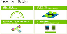
NVIDIA revealed more details of its upcoming "Pascal" GPU architecture at the Japanese edition of the Graphics Technology Conference. The architecture will be designed to nearly double performance/Watt over the current "Maxwell" architecture, by implementing the latest tech. This begins with stacked HBM2 (high-bandwidth memory 2). The top "Pascal" based product will feature four 4-gigabyte HBM2 stacks, totaling 16 GB of memory. The combined memory bandwidth for the chip will be 1 TB/s. Internally, bandwidths can touch as high as 2 TB/s. The chip itself will support up to 32 GB of memory, and so enterprise variants (Quadro, Tesla), could max out the capacity. The consumer GeForce variant is expected to serve up 16 GB.
It's also becoming clear that NVIDIA will build its "Pascal" chips on the 16 nanometer FinFET process (AMD will build its next-gen chips on more advanced 14 nm process). NVIDIA is innovating a new interconnect called NVLink, which will change the way the company has been building dual-GPU graphics cards. Currently, dual-GPU cards are essentially two graphics cards on a common PCB, with PCIe bandwidth from the slot shared by a bridge-chip, and an internal SLI bridge connecting the two GPUs. With NVLink, the two GPUs will be interconnected with an 80 GB/s bi-directional data path, letting each GPU directly address memory controlled by the other. This should greatly improve memory management in games that take advantage of newer APIs such as DirectX 12 and Vulkan; and prime the graphics card for higher display resolutions. NVIDIA is expected to launch its first "Pascal" based products in the first half of 2016.

View at TechPowerUp Main Site
It's also becoming clear that NVIDIA will build its "Pascal" chips on the 16 nanometer FinFET process (AMD will build its next-gen chips on more advanced 14 nm process). NVIDIA is innovating a new interconnect called NVLink, which will change the way the company has been building dual-GPU graphics cards. Currently, dual-GPU cards are essentially two graphics cards on a common PCB, with PCIe bandwidth from the slot shared by a bridge-chip, and an internal SLI bridge connecting the two GPUs. With NVLink, the two GPUs will be interconnected with an 80 GB/s bi-directional data path, letting each GPU directly address memory controlled by the other. This should greatly improve memory management in games that take advantage of newer APIs such as DirectX 12 and Vulkan; and prime the graphics card for higher display resolutions. NVIDIA is expected to launch its first "Pascal" based products in the first half of 2016.

View at TechPowerUp Main Site


