- Joined
- Oct 9, 2007
- Messages
- 47,647 (7.44/day)
- Location
- Dublin, Ireland
| System Name | RBMK-1000 |
|---|---|
| Processor | AMD Ryzen 7 5700G |
| Motherboard | Gigabyte B550 AORUS Elite V2 |
| Cooling | DeepCool Gammax L240 V2 |
| Memory | 2x 16GB DDR4-3200 |
| Video Card(s) | Galax RTX 4070 Ti EX |
| Storage | Samsung 990 1TB |
| Display(s) | BenQ 1440p 60 Hz 27-inch |
| Case | Corsair Carbide 100R |
| Audio Device(s) | ASUS SupremeFX S1220A |
| Power Supply | Cooler Master MWE Gold 650W |
| Mouse | ASUS ROG Strix Impact |
| Keyboard | Gamdias Hermes E2 |
| Software | Windows 11 Pro |
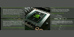
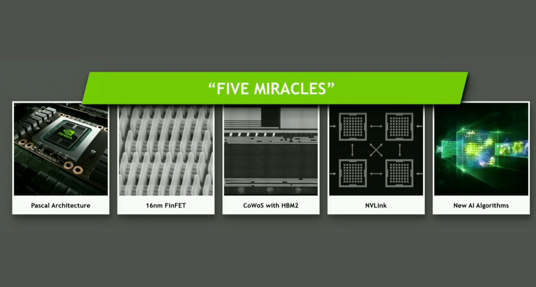
NVIDIA unveiled the Tesla P100, the first product based on the company's "Pascal" GPU architecture. At its core is a swanky new multi-chip module, similar in its essential layout to the AMD "Fiji." A 15 billion-transistor GPU die sits on top of a silicon wafer, through which a 4096-bit wide HBM2 memory interface wires it to four 3D HBM2 stacks; and with the wafer sitting on the fiberglass substrate that's rooted into the PCB over a ball-grid array. With the GPU die, wafer, and memory dies put together, this package has a cumulative transistor count of 150 billion transistors. The GPU die is built on the 16 nm FinFET process, and is 600 mm² in area.
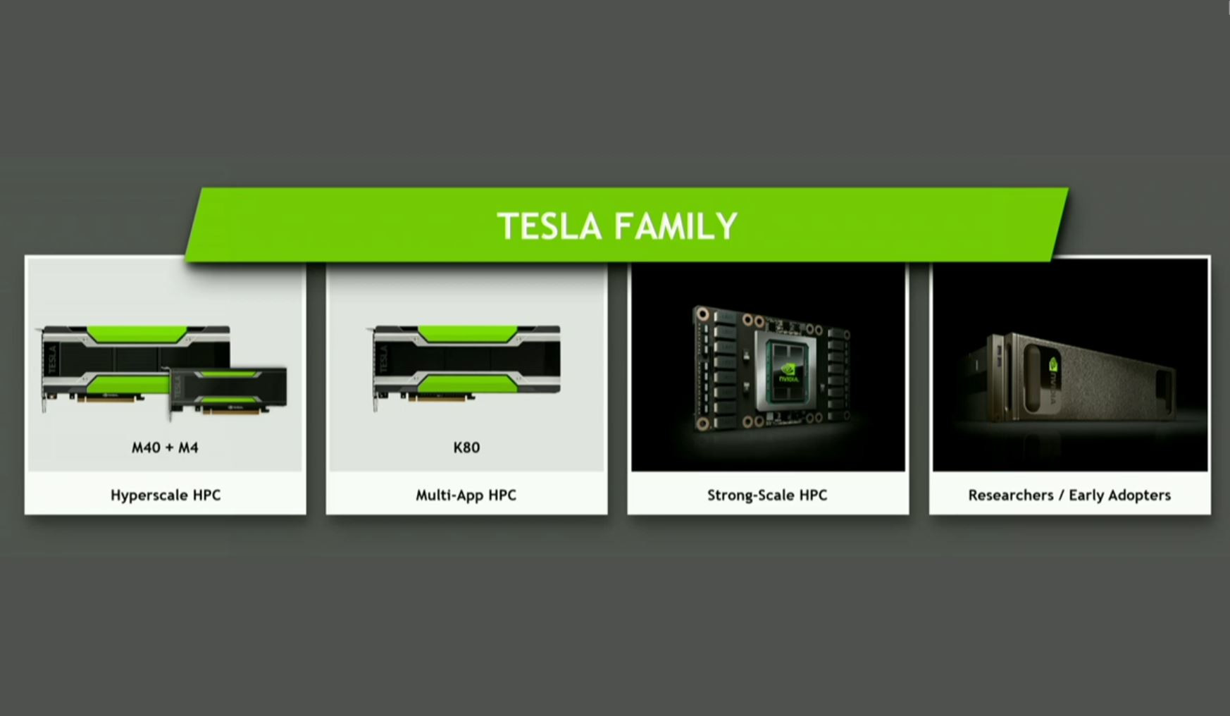
The P100 sits on top of a space-efficient PCB that looks less like a video card, and more like a compact module that can be tucked away into ultra-high density supercomputing cluster boxes, such as the new NVIDIA DGX-1. The P100 offers a double-precision (FP64) compute performance of 5.3 TFLOP/s, FP32 performance of 10.6 TFLOP/s, and FP16 performance of a whopping 21.2 TFLOP/s. The chip has registers as big as 14.2 MB, and an L2 cache of 4 MB. In addition to PCI-Express, each P100 chip will be equipped with NVLink, and in-house developed high-bandwidth interconnect by NVIDIA, with bandwidths as high as 80 GB/s per direction, 160 GB/s both directions. This allows extremely high-bandwidth paths between GPUs, so they could share memory and work more like single-GPUs. The P100 is already in volume production, with its target customers already having bought it all the way up to its OEM channel availability some time in Q1-2017.


View at TechPowerUp Main Site
Last edited:


