- Joined
- Oct 9, 2007
- Messages
- 47,537 (7.47/day)
- Location
- Hyderabad, India
| System Name | RBMK-1000 |
|---|---|
| Processor | AMD Ryzen 7 5700G |
| Motherboard | ASUS ROG Strix B450-E Gaming |
| Cooling | DeepCool Gammax L240 V2 |
| Memory | 2x 8GB G.Skill Sniper X |
| Video Card(s) | Palit GeForce RTX 2080 SUPER GameRock |
| Storage | Western Digital Black NVMe 512GB |
| Display(s) | BenQ 1440p 60 Hz 27-inch |
| Case | Corsair Carbide 100R |
| Audio Device(s) | ASUS SupremeFX S1220A |
| Power Supply | Cooler Master MWE Gold 650W |
| Mouse | ASUS ROG Strix Impact |
| Keyboard | Gamdias Hermes E2 |
| Software | Windows 11 Pro |
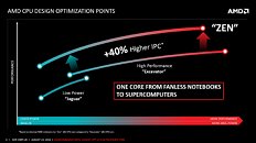
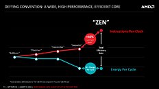
AMD Tuesday hosted a ZEN microarchitecture deep-dive presentation in the backdrop of Hot Chips, outlining its road to a massive 40 percent gain in IPC (translated roughly as per-core performance gains), over the current "Excavator" microarchitecture. The company credits the gains to three major changes with ZEN: better core engine, better cache system, and lower power. With ZEN, AMD pulled back from its "Bulldozer" approach to cores, in which two cores share certain number-crunching components to form "modules," and back to a self-sufficient core design.
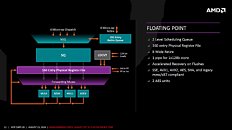
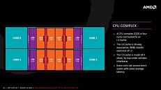
Beyond cores, the next-level subunit of the ZEN architecture is the CPU-Complex (CCX), in which four cores share an 8 MB L3 cache. This isn't different from current Intel architectures, the cores share nothing beyond L3 cache, making them truly independent. What makes ZEN a better core, besides its independence from other cores, and additional integer pipelines; subtle upscaling in key ancillaries such as micro-Op dispatch, instruction schedulers; retire, load, and store queues; and a larger quad-issue FPU.
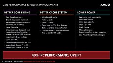
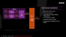
AMD also improved the cache system. The hierarchy is similar to pre-Bulldozer AMD architectures, with L3 cache being shared between full-fledged cores, and each core having a dedicated L2 cache. The L1 cache is now write-back (and not write-through), the SRAM that makes up the L2 and L3 caches are faster.
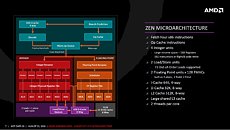
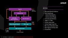
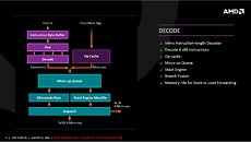
The L3 cache SRAM has 5 times higher bandwidth than the L3 cache found on current AMD architectures. The L1 and L2 caches have 2 times the bandwidth. Load from cache to FPU is now faster. The core is endowed with 64 KB each of L1I cache, 32 KB L1D cache; 512 KB of dedicated L2 cache, and 8 MB of L3 cache shared between four cores in a CCX.
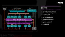
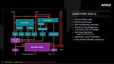
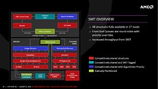
ZEN introduces simultaneous multi-threading (SMT) to AMD processors. Intel's SMT implementation is the popular HyperThreading Technology. AMD's SMT is similar in that each core is addressed to as two threads, with each thread competing for the resources on the core.
The third key area is lower-power, and this is attributed not just to the silicon-level gains yielded from the move to the 14 nm FinFET process. The design team focused on power-draw from the very inception of the ZEN core project. The L1 write-back cache, and the Op cache lower power-draw; the various components on ZEN processors feature aggressive clock-gating, although there's no power-gating.

AMD expanded the ISA CPU instruction-sets, with AVX, AVX2, BMI1, BMI2, AES, RDRAND, sMEP, SHA1/SHA256, ADX, CFLUSHopt, XSAVEC/XSAVES/XRSTORS, and SMAP. The company also introduced a few AMD-exclusive instruction sets, which can be taken advantage of for better performance, including CLzero, and PTE Coalescing.
View at TechPowerUp Main Site
Beyond cores, the next-level subunit of the ZEN architecture is the CPU-Complex (CCX), in which four cores share an 8 MB L3 cache. This isn't different from current Intel architectures, the cores share nothing beyond L3 cache, making them truly independent. What makes ZEN a better core, besides its independence from other cores, and additional integer pipelines; subtle upscaling in key ancillaries such as micro-Op dispatch, instruction schedulers; retire, load, and store queues; and a larger quad-issue FPU.


AMD also improved the cache system. The hierarchy is similar to pre-Bulldozer AMD architectures, with L3 cache being shared between full-fledged cores, and each core having a dedicated L2 cache. The L1 cache is now write-back (and not write-through), the SRAM that makes up the L2 and L3 caches are faster.


The L3 cache SRAM has 5 times higher bandwidth than the L3 cache found on current AMD architectures. The L1 and L2 caches have 2 times the bandwidth. Load from cache to FPU is now faster. The core is endowed with 64 KB each of L1I cache, 32 KB L1D cache; 512 KB of dedicated L2 cache, and 8 MB of L3 cache shared between four cores in a CCX.


ZEN introduces simultaneous multi-threading (SMT) to AMD processors. Intel's SMT implementation is the popular HyperThreading Technology. AMD's SMT is similar in that each core is addressed to as two threads, with each thread competing for the resources on the core.


The third key area is lower-power, and this is attributed not just to the silicon-level gains yielded from the move to the 14 nm FinFET process. The design team focused on power-draw from the very inception of the ZEN core project. The L1 write-back cache, and the Op cache lower power-draw; the various components on ZEN processors feature aggressive clock-gating, although there's no power-gating.

AMD expanded the ISA CPU instruction-sets, with AVX, AVX2, BMI1, BMI2, AES, RDRAND, sMEP, SHA1/SHA256, ADX, CFLUSHopt, XSAVEC/XSAVES/XRSTORS, and SMAP. The company also introduced a few AMD-exclusive instruction sets, which can be taken advantage of for better performance, including CLzero, and PTE Coalescing.
View at TechPowerUp Main Site


