Raevenlord
News Editor
- Joined
- Aug 12, 2016
- Messages
- 3,755 (1.19/day)
- Location
- Portugal
| System Name | The Ryzening |
|---|---|
| Processor | AMD Ryzen 9 5900X |
| Motherboard | MSI X570 MAG TOMAHAWK |
| Cooling | Lian Li Galahad 360mm AIO |
| Memory | 32 GB G.Skill Trident Z F4-3733 (4x 8 GB) |
| Video Card(s) | Gigabyte RTX 3070 Ti |
| Storage | Boot: Transcend MTE220S 2TB, Kintson A2000 1TB, Seagate Firewolf Pro 14 TB |
| Display(s) | Acer Nitro VG270UP (1440p 144 Hz IPS) |
| Case | Lian Li O11DX Dynamic White |
| Audio Device(s) | iFi Audio Zen DAC |
| Power Supply | Seasonic Focus+ 750 W |
| Mouse | Cooler Master Masterkeys Lite L |
| Keyboard | Cooler Master Masterkeys Lite L |
| Software | Windows 10 x64 |
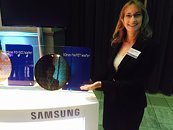
In an announcement that's sure to stir the foundry gods, Samsung Electronics, a world leader in advanced semiconductor technology, announced today that it is expanding its advanced foundry process technology offerings with the fourth-generation 14-nanometer (nm) process (14LPU) and the third-generation 10nm process (10LPU). The announcement comes as Samsung increases investment so as to meet the requirements of next generation products, ranging from mobile and consumer electronics (Snapdragon 830 and Samsung's own Exynos 8895 come to mind) to data centers and automotives.
Ben Suh, Senior Vice President of foundry marketing at Samsung Electronics, issued the following statement: "After we announced the industry's first 10nm mass production in mid-October, we have now also expanded our lineup with new foundry offerings, 14LPU and 10LPU. Samsung is very confident with our technology definitions that provide design advantages on an aggressive process with manufacturability considerations. We have received tremendous positive market feedback and are looking forward to expanding our leadership in the advanced process technology space."

Samsung's third-generation 10nm process, 10LPU, will provide further area reduction compared to its previous generations (10LPE and 10LPP). Due to limitations of current lithography technologies, 10LPU is expected to be the most cost-effective cutting-edge process technology in the industry for a yet indeterminate amount of time. On top of the new process offerings, Samsung also updated its 7nm EUV process development status and showcased its 7nm EUV wafer - though the technology is still some time away from mass production.Together with the second-generation 10nm process (10LPP) that offers an extra performance boost from 10LPE, 10LPU is positioned to meet the needs of an extended range of applications that can benefit from the advanced 10nm process.
View at TechPowerUp Main Site
Ben Suh, Senior Vice President of foundry marketing at Samsung Electronics, issued the following statement: "After we announced the industry's first 10nm mass production in mid-October, we have now also expanded our lineup with new foundry offerings, 14LPU and 10LPU. Samsung is very confident with our technology definitions that provide design advantages on an aggressive process with manufacturability considerations. We have received tremendous positive market feedback and are looking forward to expanding our leadership in the advanced process technology space."

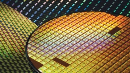
Samsung's third-generation 10nm process, 10LPU, will provide further area reduction compared to its previous generations (10LPE and 10LPP). Due to limitations of current lithography technologies, 10LPU is expected to be the most cost-effective cutting-edge process technology in the industry for a yet indeterminate amount of time. On top of the new process offerings, Samsung also updated its 7nm EUV process development status and showcased its 7nm EUV wafer - though the technology is still some time away from mass production.Together with the second-generation 10nm process (10LPP) that offers an extra performance boost from 10LPE, 10LPU is positioned to meet the needs of an extended range of applications that can benefit from the advanced 10nm process.
View at TechPowerUp Main Site
