- Joined
- Oct 9, 2007
- Messages
- 47,402 (7.52/day)
- Location
- Hyderabad, India
| System Name | RBMK-1000 |
|---|---|
| Processor | AMD Ryzen 7 5700G |
| Motherboard | ASUS ROG Strix B450-E Gaming |
| Cooling | DeepCool Gammax L240 V2 |
| Memory | 2x 8GB G.Skill Sniper X |
| Video Card(s) | Palit GeForce RTX 2080 SUPER GameRock |
| Storage | Western Digital Black NVMe 512GB |
| Display(s) | BenQ 1440p 60 Hz 27-inch |
| Case | Corsair Carbide 100R |
| Audio Device(s) | ASUS SupremeFX S1220A |
| Power Supply | Cooler Master MWE Gold 650W |
| Mouse | ASUS ROG Strix Impact |
| Keyboard | Gamdias Hermes E2 |
| Software | Windows 11 Pro |
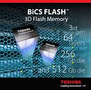
Toshiba Corporation has today unveiled the latest addition in its industry-leading line-up of BiCS FLASH three-dimensional flash memory with a stacked cell structure, a 64-layer device that achieves a 512-gigabit (64-gigabytes) capacity with 3-bit-per-cell (triple-level cell, TLC) technology. The new device will be used in applications that include enterprise and consumer SSD. Sample shipments of the chip started this month, and mass production is scheduled for the second half of this calendar year.
Toshiba continues to refine BiCS FLASH, and the next milestone on its development roadmap is the industry's largest capacity, a 1-terabyte product with a 16-die stacked architecture in a single package. Plans call for the start of sample shipments in April 2017. For the new 512-gigabit device, Toshiba deployed leading-edge 64-layer stacking process to realize a 65% larger capacity per unit chip size than the 48-layer 256-gigabit (32-gigabytes) device, and has increased memory capacity per silicon wafer, reducing the cost per bit.

Toshiba's Memory business already mass produces 64-layer 256-gigabit (32-gigabytes) devices and will expand BiCS FLASH production. It will advance 3D technology to realize increased densities and finer processes in order to meet diversifying market needs.
View at TechPowerUp Main Site
Toshiba continues to refine BiCS FLASH, and the next milestone on its development roadmap is the industry's largest capacity, a 1-terabyte product with a 16-die stacked architecture in a single package. Plans call for the start of sample shipments in April 2017. For the new 512-gigabit device, Toshiba deployed leading-edge 64-layer stacking process to realize a 65% larger capacity per unit chip size than the 48-layer 256-gigabit (32-gigabytes) device, and has increased memory capacity per silicon wafer, reducing the cost per bit.

Toshiba's Memory business already mass produces 64-layer 256-gigabit (32-gigabytes) devices and will expand BiCS FLASH production. It will advance 3D technology to realize increased densities and finer processes in order to meet diversifying market needs.
View at TechPowerUp Main Site


