Raevenlord
News Editor
- Joined
- Aug 12, 2016
- Messages
- 3,755 (1.20/day)
- Location
- Portugal
| System Name | The Ryzening |
|---|---|
| Processor | AMD Ryzen 9 5900X |
| Motherboard | MSI X570 MAG TOMAHAWK |
| Cooling | Lian Li Galahad 360mm AIO |
| Memory | 32 GB G.Skill Trident Z F4-3733 (4x 8 GB) |
| Video Card(s) | Gigabyte RTX 3070 Ti |
| Storage | Boot: Transcend MTE220S 2TB, Kintson A2000 1TB, Seagate Firewolf Pro 14 TB |
| Display(s) | Acer Nitro VG270UP (1440p 144 Hz IPS) |
| Case | Lian Li O11DX Dynamic White |
| Audio Device(s) | iFi Audio Zen DAC |
| Power Supply | Seasonic Focus+ 750 W |
| Mouse | Cooler Master Masterkeys Lite L |
| Keyboard | Cooler Master Masterkeys Lite L |
| Software | Windows 10 x64 |
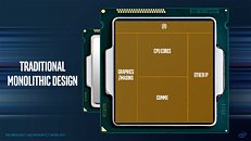
Rumors have been making the rounds about an as-of-yet unannounced product from Intel: a Kaby Lake-G series which would mark Intel's return foray to a multi-chip module in a singular package. The company has already played with such a design before with its Clarkdale family of processors - which married a 32 nm CPU as well as a 45 nm GPU and memory controller in a single package. Kaby Lake-G will reportedly make away with its simple, low-data rate implementation and communication between two parts, instead carrying itself on the shoulders of Intel's EMIB (Embedded Multi-die Interconnect Bridge), which the company claims is a "more elegant interconnect for a more civilized age."
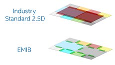
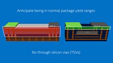
Instead of using a large silicon interposer typically found in other 2.5D approaches (like AMD did whilst marrying its Fiji dies with HBM memory), EMIB uses a very small bridge die, with multiple routing layers, which provide a good measure of price/data paths for the interconnected, heterogeneous architecture. This saves on the costly TSV (Through-Silicon Vias) that dot the interposer approach.
For now, rumors peg these Kaby Lake-G as special BGA processors based on Kaby Lake, with an additional discrete GPU on the package. The TDP of these processors (at 65 W and 100 W) is well above the Kaby Lake-H's known 45 Watts. Which begs the question: what exactly is under the hood? This, including Intel's modular approach to chip design for which it developed its EMIB technology, could probably account for the AMD graphic's chip TDP - a discrete-level GPU which would be integrated on-die, EMIB's routing layers handling the data exchange between GPU and processor. This is where HBM 2 memory integration would also come in, naturally - a way to keep a considerable amount of high-speed memory inside the package, accessible by the silicon slices that would need to. Nothing in the leaked information seems to point towards this HBM 2 integration, however.

Also helping these "AMD Radeon IP integration" story (besides TDP) is that the two chips that will be part of the Kaby Lake-G series will feature a package size of 58.5 x 31mm - bigger than a desktop Kaby Lake-S (37.5 x 37.5 mm) and the Kaby Lake-H series chips (42 x 28mm). The extra space would accommodate increased footprint of the GPU package - though for now, leaked information points only, again, to Intel's own GT2 graphics solution, though Benchlife seems to put much stock on the AMD side of the equation.
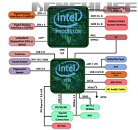
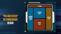
The heterogeneous, modular approach to CPU development here would really benefit Intel thusly: it would allow it to integrate such external graphics solutions that could be produced in other factories entirely and then fitted onto the package; would allow Intel to save die space on their 10 nm dies for actual cores, increasing yields from their 10 nm process; and would allow Intel to recycle old processes with new logic inside the CPU package, permitting the company to better distribute production load across different processes, better utilizing (and extracting value from) their not-so-state-of-the-art processes.
If Intel advances with this modular approach, we stand to see some really interesting designs, with multiple manufacturing processes working in tandem inside a single package, giving Intel more flexibility in developing and implementing its fabrication processes. What do you think about this take on CPU development?
View at TechPowerUp Main Site
Instead of using a large silicon interposer typically found in other 2.5D approaches (like AMD did whilst marrying its Fiji dies with HBM memory), EMIB uses a very small bridge die, with multiple routing layers, which provide a good measure of price/data paths for the interconnected, heterogeneous architecture. This saves on the costly TSV (Through-Silicon Vias) that dot the interposer approach.


For now, rumors peg these Kaby Lake-G as special BGA processors based on Kaby Lake, with an additional discrete GPU on the package. The TDP of these processors (at 65 W and 100 W) is well above the Kaby Lake-H's known 45 Watts. Which begs the question: what exactly is under the hood? This, including Intel's modular approach to chip design for which it developed its EMIB technology, could probably account for the AMD graphic's chip TDP - a discrete-level GPU which would be integrated on-die, EMIB's routing layers handling the data exchange between GPU and processor. This is where HBM 2 memory integration would also come in, naturally - a way to keep a considerable amount of high-speed memory inside the package, accessible by the silicon slices that would need to. Nothing in the leaked information seems to point towards this HBM 2 integration, however.

Also helping these "AMD Radeon IP integration" story (besides TDP) is that the two chips that will be part of the Kaby Lake-G series will feature a package size of 58.5 x 31mm - bigger than a desktop Kaby Lake-S (37.5 x 37.5 mm) and the Kaby Lake-H series chips (42 x 28mm). The extra space would accommodate increased footprint of the GPU package - though for now, leaked information points only, again, to Intel's own GT2 graphics solution, though Benchlife seems to put much stock on the AMD side of the equation.

The heterogeneous, modular approach to CPU development here would really benefit Intel thusly: it would allow it to integrate such external graphics solutions that could be produced in other factories entirely and then fitted onto the package; would allow Intel to save die space on their 10 nm dies for actual cores, increasing yields from their 10 nm process; and would allow Intel to recycle old processes with new logic inside the CPU package, permitting the company to better distribute production load across different processes, better utilizing (and extracting value from) their not-so-state-of-the-art processes.
If Intel advances with this modular approach, we stand to see some really interesting designs, with multiple manufacturing processes working in tandem inside a single package, giving Intel more flexibility in developing and implementing its fabrication processes. What do you think about this take on CPU development?
View at TechPowerUp Main Site


