- Joined
- Oct 9, 2007
- Messages
- 47,435 (7.51/day)
- Location
- Hyderabad, India
| System Name | RBMK-1000 |
|---|---|
| Processor | AMD Ryzen 7 5700G |
| Motherboard | ASUS ROG Strix B450-E Gaming |
| Cooling | DeepCool Gammax L240 V2 |
| Memory | 2x 8GB G.Skill Sniper X |
| Video Card(s) | Palit GeForce RTX 2080 SUPER GameRock |
| Storage | Western Digital Black NVMe 512GB |
| Display(s) | BenQ 1440p 60 Hz 27-inch |
| Case | Corsair Carbide 100R |
| Audio Device(s) | ASUS SupremeFX S1220A |
| Power Supply | Cooler Master MWE Gold 650W |
| Mouse | ASUS ROG Strix Impact |
| Keyboard | Gamdias Hermes E2 |
| Software | Windows 11 Pro |
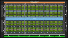
NVIDIA at the GTC 2017 event, announced its next-generation "Volta" GPU architecture. As with its current "Pascal" architecture, "Volta" was unveiled in its biggest, most feature-rich implementation, the Tesla V100 HPC board, driven by the GV100 silicon. Given the HPC applications of NVIDIA's Tesla family of products, the GV100 has certain components that won't make it to the consumer GeForce family. Despite these, the GV100 is the pinnacle of NVIDIA's silicon engineering. According to the GPU block diagram released by the company, the GV100 has a similar component hierarchy to previous-generation NVIDIA chips, with some major changes to its basic number-crunching machinery, the streaming multiprocessor (SM).
The "Volta" streaming multiprocessor (SM) on the GV100 silicon features both FP32 and FP64 CUDA cores. Consumer graphics implementations of "Volta" which drive future GeForce products could lack those specialized FP64 cores. Each SM features 64 FP32 CUDA cores, and 32 FP64 cores. The FP64 cores can handle 32-bit, 16-bit, and even primitive 8-bit operations. The GV100 features 80 SMs, so you're looking at 5,120 FP32 and 2,560 FP64 CUDA cores. In addition, Volta introduces a component called Tensor cores, specialized machinery designed to speed up deep-learning training and neural net building. An SM has 8 of these, so the GV100 has 640. As with FP64 cores, Tensor cores may not make it to consumer-graphics implementations. Given its SM count, the GV100 features 320 TMUs. NVIDIA clocked the GV100 to run at 1455 MHz boost.


The Tesla V100 is advertised to offer 50% higher FP32 and FP64 peak performance over the "Pascal" based Tesla P100. Its peak FP32 throughput is rated at 15 TFLOP/s, with 7.5 TFLOP/s FP64 peak throughput. The Tensor cores "effectively" run at 120 TFLOP/s to perform their very specialized task of training deep-learning neural nets. These components feature matrix-matrix multiplication units, which is a key math operation in neural net training. They accelerate neural net building/training by 12X.

Built on the new 12 nanometer process, the GV100 is a multi-chip module with a large, 815 mm² GPU die, with a gargantuan transistor-count of 21.1 billion, neighbored by four 32 Gbit HBM2 memory stacks, which make up 16 GB of memory. These stacks interface with the GV100 over a 4096-bit wide memory interface, through a silicon interposer. At 1 GHz, this memory setup could cushion the GV100 with a memory bandwidth of 1 TB/s. HBM2 could still be exclusive to the Tesla family of products in NVIDIA's product-stack, as it continues to be expensive to implement in the consumer-segment for NVIDIA. Besides FP64 and Tensor cores, consumer implementations of "Volta" could feature inexpensive yet suitably fast GDDR6 memory. One of the pioneering manufacturers of HBM, SK Hynix, even demonstrated GDDR6 at GTC, so unless NVIDIA is fighting for its life in performance against AMD, we expect it to stick to GDDR6 in the consumer segment.

The Tesla V100 HPC card will be developed in two packages - integrated boards with NVLink interface for more high-density farm builds, and add-on card with PCI-Express interface for workstations. It will be sold through specialized retail channels.
View at TechPowerUp Main Site
The "Volta" streaming multiprocessor (SM) on the GV100 silicon features both FP32 and FP64 CUDA cores. Consumer graphics implementations of "Volta" which drive future GeForce products could lack those specialized FP64 cores. Each SM features 64 FP32 CUDA cores, and 32 FP64 cores. The FP64 cores can handle 32-bit, 16-bit, and even primitive 8-bit operations. The GV100 features 80 SMs, so you're looking at 5,120 FP32 and 2,560 FP64 CUDA cores. In addition, Volta introduces a component called Tensor cores, specialized machinery designed to speed up deep-learning training and neural net building. An SM has 8 of these, so the GV100 has 640. As with FP64 cores, Tensor cores may not make it to consumer-graphics implementations. Given its SM count, the GV100 features 320 TMUs. NVIDIA clocked the GV100 to run at 1455 MHz boost.


The Tesla V100 is advertised to offer 50% higher FP32 and FP64 peak performance over the "Pascal" based Tesla P100. Its peak FP32 throughput is rated at 15 TFLOP/s, with 7.5 TFLOP/s FP64 peak throughput. The Tensor cores "effectively" run at 120 TFLOP/s to perform their very specialized task of training deep-learning neural nets. These components feature matrix-matrix multiplication units, which is a key math operation in neural net training. They accelerate neural net building/training by 12X.

Built on the new 12 nanometer process, the GV100 is a multi-chip module with a large, 815 mm² GPU die, with a gargantuan transistor-count of 21.1 billion, neighbored by four 32 Gbit HBM2 memory stacks, which make up 16 GB of memory. These stacks interface with the GV100 over a 4096-bit wide memory interface, through a silicon interposer. At 1 GHz, this memory setup could cushion the GV100 with a memory bandwidth of 1 TB/s. HBM2 could still be exclusive to the Tesla family of products in NVIDIA's product-stack, as it continues to be expensive to implement in the consumer-segment for NVIDIA. Besides FP64 and Tensor cores, consumer implementations of "Volta" could feature inexpensive yet suitably fast GDDR6 memory. One of the pioneering manufacturers of HBM, SK Hynix, even demonstrated GDDR6 at GTC, so unless NVIDIA is fighting for its life in performance against AMD, we expect it to stick to GDDR6 in the consumer segment.

The Tesla V100 HPC card will be developed in two packages - integrated boards with NVLink interface for more high-density farm builds, and add-on card with PCI-Express interface for workstations. It will be sold through specialized retail channels.
View at TechPowerUp Main Site


