- Joined
- Oct 9, 2007
- Messages
- 47,417 (7.51/day)
- Location
- Hyderabad, India
| System Name | RBMK-1000 |
|---|---|
| Processor | AMD Ryzen 7 5700G |
| Motherboard | ASUS ROG Strix B450-E Gaming |
| Cooling | DeepCool Gammax L240 V2 |
| Memory | 2x 8GB G.Skill Sniper X |
| Video Card(s) | Palit GeForce RTX 2080 SUPER GameRock |
| Storage | Western Digital Black NVMe 512GB |
| Display(s) | BenQ 1440p 60 Hz 27-inch |
| Case | Corsair Carbide 100R |
| Audio Device(s) | ASUS SupremeFX S1220A |
| Power Supply | Cooler Master MWE Gold 650W |
| Mouse | ASUS ROG Strix Impact |
| Keyboard | Gamdias Hermes E2 |
| Software | Windows 11 Pro |
It has been a huge weekend of product announcements and launches from AMD, which expanded not just its client computing CPU lineup on both ends, but also expanded its Radeon graphics cards family with both client- and professional-segment graphics cards. This article provides a brief summary of everything AMD launched or announced today, with their possible market-availability dates.

AMD Radeon RX Vega Family
AMD today finally announced its Radeon RX Vega family of performance-segment consumer graphics cards, based on its new 14 nm "Vega 10" ASIC, which combines a large GPU die with two 32 Gbit HBM2 memory stacks, totaling 8 GB of memory; sitting on a silicon interposer. The company announced five SKUs based on this ASIC:
The Radeon Pro WX 9100 is a professional graphics card, which is differentiated from the Radeon Pro Vega Frontier Edition, even though the two feature the same exact underlying GPU. It features an engine clock of 1500 MHz, a memory bandwidth of 484 GB/s, and 16 GB of memory. The display output layout is slightly different, with six mini-DisplayPort 1.4 connectors, and rear-positioned power inputs of 6-pin + 8-pin. The difference here is the Radeon Pro driver, and an exhaustive 7-year product warranty, and premium after-sales support. The card is priced at USD $2,199.
The new-generation Radeon Pro SSG combines the 16 GB HBM2 high-bandwidth cache of a Radeon Pro WX 9100 with 1 TB of NVMe NAND flash memory on the card (an SSD); and the ability to treat it as video memory, by juggling hot-data (most frequently accessed data) in and out of this NAND flash, onto the HBM2 high-bandwidth cache. This allows content creators to deal with gargantuan data-sets that reside in the graphics card, and AMD has shown demos to prove that such an arrangement improves workflow and processing times significantly, which enables the company to ask a lofty $6,999 for this card, backed by the same 7-year warranty.
AMD Ryzen 3 Family Availability
AMD expanded the lower-end of its socket AM4 Ryzen desktop processor family with the Ryzen 3 series, which are now available in the retail channel. The quad-core Ryzen 3 1300X, with clock speeds of 3.40 GHz, and 3.70 GHz boost, with XFR that cranks clock speeds up to 3.90 GHz; is priced at $129. Its more affordable sibling, the quad-core Ryzen 3 1200, which is clocked at 3.10 GHz, with 3.40 GHz boost, and a tiny 50 MHz XFR; is priced at $109. Both chips are endowed with 8 MB of L3 cache.
Ryzen Threadripper HEDT Processors
AMD announced its first true HEDT (high-end desktop) processors in a decade, with the Ryzen Threadripper series. Designed to compete with Intel Core X family, these chips offer a large amount of CPU cores backed by SMT; with double the memory bus width, and double the PCI-Express lane budget; enabling desktops with multiple bandwidth-hungry devices such as graphics cards and SSDs; and large amounts of memory. These chips are built in the new TR4 package; and are being launched alongside compatible motherboards based on the AMD X399 chipset. The lineup is as follows:
NVIDIA is selling turnkey deep-learning and HPC boxes that combine its Tesla HPC cards with Intel Xeon processors, so researchers don't have to bother about which system to build. AMD wants a slice of that market, and hence unveiled Project 47, marketed as AMD P47 Petaflop Rack, promising 1000 TFLOP/s of compute power in a standard size rack.
The P47 combines twenty (20) AMD EPYC 7601 32-core processors, with eighty (80!) Radeon Vega Instinct GPUs, and twenty Mellanox-made 100 Gb InfinityBand cards, and 10 TB of Samsung NVMe storage. to belt out 1 PFLOP/s of peak single-precision compute performance, 2 PFLOP/s of half-precision (FP16) performance, at 30 GLOP/s per Watt single-precision. The company didn't reveal pricing, however we expect it to be on par with that of a luxury sedan.
View at TechPowerUp Main Site


AMD Radeon RX Vega Family
AMD today finally announced its Radeon RX Vega family of performance-segment consumer graphics cards, based on its new 14 nm "Vega 10" ASIC, which combines a large GPU die with two 32 Gbit HBM2 memory stacks, totaling 8 GB of memory; sitting on a silicon interposer. The company announced five SKUs based on this ASIC:
- Radeon RX Vega 64 Liquid Cooled Edition: This is a reference-design Radeon RX Vega 64, featuring a full-featured "Vega 10" ASIC, mated with an all-in-one liquid cooling solution, much like the R9 Fury X. Taking advantage of the liquid-cooling, AMD clocked the chip higher. The "Vega 10" silicon features 64 next-generation compute units (NGCUs), totaling 4,096 stream processors, 256 TMUs, 64 ROPs, and a 2048-bit wide HBM2 memory interface. On the RX Vega 64 Liquid Cooled Edition (LCE), the GPU is clocked at 1406 MHz, with 1677 MHz boost. Due to the higher clocks, the TDP of this card is rated higher, at 345W. It draws power from two 8-pin PCIe power connectors. The memory bandwidth of this SKU is 484 GB/s. The pricing of this SKU is unknown at this point.
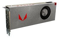
- Radeon RX Vega 64 Limited Edition: This is a premium reference-design SKU of the RX Vega 64, which is air-cooled, and sticks to AMD's reference clocks. The air-cooling solution features a premium brushed aluminium shroud and matching back-plate, with illuminated "R" corner logo cube, the Vega logo, and the Radeon logo on the top. The GPU is clocked at 1247 MHz, with 1546 MHz boost, and an untouched memory bandwidth of 484 GB/s. Owing to its lower clocks, its TDP is rated at 295W. The pricing of this SKU, too, remains unknown.
- Radeon RX Vega 64 (reference): This is the reference-design RX Vega, which will be widely available. It has the same clock speeds as the RX Vega 64 Limited Edition, but a simpler plastic+steel reference-design cooling solution. The underlying heatsink and 30 mm fan remain the same, although the cooler shroud is made of the same plastic and steel as the reference RX 580. This SKU is for early adopters of the card, and will be priced at USD $499, when it hits the shelves mid-August. AMD pins its performance somewhere between the GeForce GTX 1070 and GTX 1080, while being closer to the latter.
- Radeon RX Vega 56: This is the smaller, more affordable sibling of the RX Vega 64. Its brand extension "56" denotes a compute unit count of 56, which works out to 3,584 stream processors. This chip will be endowed with 192 TMUs, 64 ROPs, and 8 GB of 2048-bit HBM2 memory. The card is clocked slightly lower than its sibling, at 1156 MHz core, 1471 MHz boost, and a slightly lower memory clock, resulting in 410 GB/s of memory bandwidth. The TDP of this card is lower still, at around 210W. At a price of $399, the RX Vega 56 could lock horns with the GTX 1070, which it's available by late-August.
- Radeon RX Vega Nano: The "Vega 10" ASIC is smaller than even the "Fiji" ASIC which powered the original Radeon R9 Nano, so this was only bound to happen. The Radeon RX Vega Nano retains the super-compact dimensions of its ancestor, while packing a full-featured "Vega 10" ASIC, but with lower clocks and more aggressive power-management. What it gives you in return, is the fastest SFF graphics card money can buy (which could come at a premium).
The Radeon Pro WX 9100 is a professional graphics card, which is differentiated from the Radeon Pro Vega Frontier Edition, even though the two feature the same exact underlying GPU. It features an engine clock of 1500 MHz, a memory bandwidth of 484 GB/s, and 16 GB of memory. The display output layout is slightly different, with six mini-DisplayPort 1.4 connectors, and rear-positioned power inputs of 6-pin + 8-pin. The difference here is the Radeon Pro driver, and an exhaustive 7-year product warranty, and premium after-sales support. The card is priced at USD $2,199.
The new-generation Radeon Pro SSG combines the 16 GB HBM2 high-bandwidth cache of a Radeon Pro WX 9100 with 1 TB of NVMe NAND flash memory on the card (an SSD); and the ability to treat it as video memory, by juggling hot-data (most frequently accessed data) in and out of this NAND flash, onto the HBM2 high-bandwidth cache. This allows content creators to deal with gargantuan data-sets that reside in the graphics card, and AMD has shown demos to prove that such an arrangement improves workflow and processing times significantly, which enables the company to ask a lofty $6,999 for this card, backed by the same 7-year warranty.
AMD Ryzen 3 Family Availability
AMD expanded the lower-end of its socket AM4 Ryzen desktop processor family with the Ryzen 3 series, which are now available in the retail channel. The quad-core Ryzen 3 1300X, with clock speeds of 3.40 GHz, and 3.70 GHz boost, with XFR that cranks clock speeds up to 3.90 GHz; is priced at $129. Its more affordable sibling, the quad-core Ryzen 3 1200, which is clocked at 3.10 GHz, with 3.40 GHz boost, and a tiny 50 MHz XFR; is priced at $109. Both chips are endowed with 8 MB of L3 cache.
Ryzen Threadripper HEDT Processors
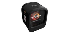
AMD announced its first true HEDT (high-end desktop) processors in a decade, with the Ryzen Threadripper series. Designed to compete with Intel Core X family, these chips offer a large amount of CPU cores backed by SMT; with double the memory bus width, and double the PCI-Express lane budget; enabling desktops with multiple bandwidth-hungry devices such as graphics cards and SSDs; and large amounts of memory. These chips are built in the new TR4 package; and are being launched alongside compatible motherboards based on the AMD X399 chipset. The lineup is as follows:
- AMD Ryzen Threadripper 1950X: This is AMD's flagship client processor. Endowed with 16 cores and 32 threads enabled by SMT; the chip features clock speeds of 3.40 GHz, and 4.00 GHz boost, and XFR adding 200 MHz further to the boost clock. It also features 32 MB of L3 cache. Available from 10th August, it is priced at USD $999.
- AMD Ryzen Threadripper 1920X: The second-best Threadripper chip you can buy at $799, when it comes out on the 10th of August, the 1920X is a 12-core/24-thread chip clocked at 3.50 GHz, and 4.00 GHz boost, with XFR adding another 200 MHz. It features an untouched 32 MB of L3 cache, and features the full 64-lane PCI-Express root complex, and quad-channel DDR4 memory interface.
- AMD Ryzen Threadripper 1900X: This is a surprising SKU. It offers 8 cores and 16 threads, and has been carved out by disabling 2 cores per CCX, per die. You still get the full quad-channel DDR4 memory interface, and 64-lane PCIe. It's also the highest-clocked Threadripper, ticking at 3.80 GHz, with 4.00 GHz boost, and XFR adding another 200 MHz. The chip is priced at $549, $50 more than the socket AM4 Ryzen 7 1800X. You pay $50 more (besides a pricier motherboard) for double the memory bus width and PCIe lane budget, which is the bargain AMD seems to be driving. The chip will be available from 31st August.
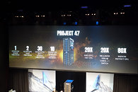
NVIDIA is selling turnkey deep-learning and HPC boxes that combine its Tesla HPC cards with Intel Xeon processors, so researchers don't have to bother about which system to build. AMD wants a slice of that market, and hence unveiled Project 47, marketed as AMD P47 Petaflop Rack, promising 1000 TFLOP/s of compute power in a standard size rack.
The P47 combines twenty (20) AMD EPYC 7601 32-core processors, with eighty (80!) Radeon Vega Instinct GPUs, and twenty Mellanox-made 100 Gb InfinityBand cards, and 10 TB of Samsung NVMe storage. to belt out 1 PFLOP/s of peak single-precision compute performance, 2 PFLOP/s of half-precision (FP16) performance, at 30 GLOP/s per Watt single-precision. The company didn't reveal pricing, however we expect it to be on par with that of a luxury sedan.
View at TechPowerUp Main Site
Last edited:


