- Joined
- Oct 9, 2007
- Messages
- 47,850 (7.39/day)
- Location
- Dublin, Ireland
| System Name | RBMK-1000 |
|---|---|
| Processor | AMD Ryzen 7 5700G |
| Motherboard | Gigabyte B550 AORUS Elite V2 |
| Cooling | DeepCool Gammax L240 V2 |
| Memory | 2x 16GB DDR4-3200 |
| Video Card(s) | Galax RTX 4070 Ti EX |
| Storage | Samsung 990 1TB |
| Display(s) | BenQ 1440p 60 Hz 27-inch |
| Case | Corsair Carbide 100R |
| Audio Device(s) | ASUS SupremeFX S1220A |
| Power Supply | Cooler Master MWE Gold 650W |
| Mouse | ASUS ROG Strix Impact |
| Keyboard | Gamdias Hermes E2 |
| Software | Windows 11 Pro |
Intel is making progress in its development of a new discrete GPU architecture, after its failed attempt with "Larrabee" that ended up as an HPC accelerator; and ancient attempts such as the i740. This comes in the wake of the company's high-profile hiring of Raja Koduri, AMD's former Radeon Technologies Group (RTG) head. The company unveiled slides pointing to the direction in which its GPU development is headed, at the IEEE International Solid-State Circuits Conference (ISSCC) in San Francisco. That direction is essentially scaling up its existing iGPU architecture, and bolstering it with mechanisms to sustain high clock speeds better.
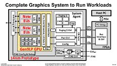
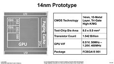
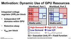
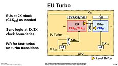
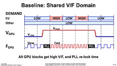
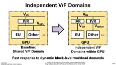
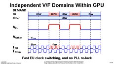
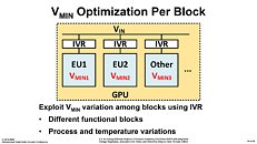
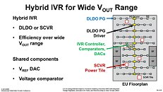
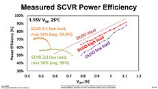
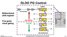
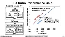
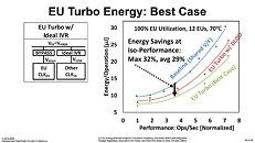
The company's first 14 nm dGPU prototype, shown as a test-chip at the ISSCC, is a 2-chip solution. The first chip contains two key components, the GPU itself, and a system agent; and the second chip is an FPGA that interfaces with the system bus. The GPU component, as it stands now, is based on Intel's Gen 9 architecture, and features a three execution unit (EU) clusters. Don't derive numbers from this yet, as Intel is only trying to demonstrate a proof of concept. The three clusters are wired to a sophisticated power/clock management mechanism that efficiently manages power and clock-speed of each individual EU. There's also a double-clock mechanism that doubles clock speeds (of the boost state) beyond what today's Gen 9 EUs can handle on Intel iGPUs. Once a suitable level of energy efficiency is achieved, Intel will use newer generations of EUs, and scale up EU counts taking advantage of newer fab processes, to develop bigger discrete GPUs.
More slides follow.



View at TechPowerUp Main Site
The company's first 14 nm dGPU prototype, shown as a test-chip at the ISSCC, is a 2-chip solution. The first chip contains two key components, the GPU itself, and a system agent; and the second chip is an FPGA that interfaces with the system bus. The GPU component, as it stands now, is based on Intel's Gen 9 architecture, and features a three execution unit (EU) clusters. Don't derive numbers from this yet, as Intel is only trying to demonstrate a proof of concept. The three clusters are wired to a sophisticated power/clock management mechanism that efficiently manages power and clock-speed of each individual EU. There's also a double-clock mechanism that doubles clock speeds (of the boost state) beyond what today's Gen 9 EUs can handle on Intel iGPUs. Once a suitable level of energy efficiency is achieved, Intel will use newer generations of EUs, and scale up EU counts taking advantage of newer fab processes, to develop bigger discrete GPUs.


More slides follow.


View at TechPowerUp Main Site


