- Joined
- Oct 9, 2007
- Messages
- 47,649 (7.44/day)
- Location
- Dublin, Ireland
| System Name | RBMK-1000 |
|---|---|
| Processor | AMD Ryzen 7 5700G |
| Motherboard | Gigabyte B550 AORUS Elite V2 |
| Cooling | DeepCool Gammax L240 V2 |
| Memory | 2x 16GB DDR4-3200 |
| Video Card(s) | Galax RTX 4070 Ti EX |
| Storage | Samsung 990 1TB |
| Display(s) | BenQ 1440p 60 Hz 27-inch |
| Case | Corsair Carbide 100R |
| Audio Device(s) | ASUS SupremeFX S1220A |
| Power Supply | Cooler Master MWE Gold 650W |
| Mouse | ASUS ROG Strix Impact |
| Keyboard | Gamdias Hermes E2 |
| Software | Windows 11 Pro |
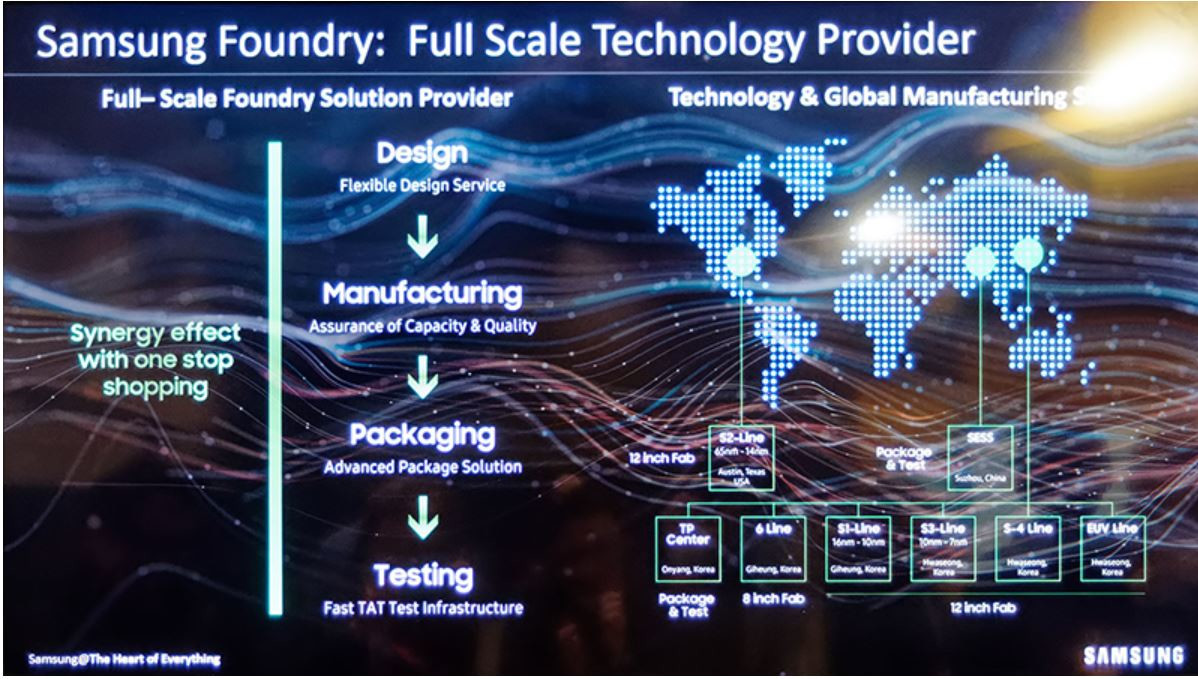
NVIDIA will implement the 7 nanometer EUV (extreme ultraviolet) lithography to build its future generation of GPUs slated for 2020, according to Japanese publication MyNavi.jp. The GPU giant could be among the first customers besides IBM, to contract Samsung for 7 nm EUV mass-production of GPUs. IBM will use the Korean semiconductor giant for manufacturing Z-series processors and FPGAs. Samsung announced in October 2018 that it will begin risk-production on its 7 nm EUV node in early-2019.
An earlier report from 2018 also forecast NVIDIA implementing 7 nm DUV (deep ultraviolet) node of TSMC for its 2019 GPU lineup. With news of the company now working with Samsung on 7 nm EUV for 2020, this seems less likely. It's possible that NVIDIA could somehow split its next generation GPU lineup between TSMC 7 nm DUV and Samsung 7 nm EUV, with the latter being used for chips with higher transistor-counts, taking advantage of the node's higher deliverable transistor densities.
View at TechPowerUp Main Site

 ...
...