- Joined
- Oct 9, 2007
- Messages
- 47,528 (7.48/day)
- Location
- Hyderabad, India
| System Name | RBMK-1000 |
|---|---|
| Processor | AMD Ryzen 7 5700G |
| Motherboard | ASUS ROG Strix B450-E Gaming |
| Cooling | DeepCool Gammax L240 V2 |
| Memory | 2x 8GB G.Skill Sniper X |
| Video Card(s) | Palit GeForce RTX 2080 SUPER GameRock |
| Storage | Western Digital Black NVMe 512GB |
| Display(s) | BenQ 1440p 60 Hz 27-inch |
| Case | Corsair Carbide 100R |
| Audio Device(s) | ASUS SupremeFX S1220A |
| Power Supply | Cooler Master MWE Gold 650W |
| Mouse | ASUS ROG Strix Impact |
| Keyboard | Gamdias Hermes E2 |
| Software | Windows 11 Pro |
At its CES 2019 keynote, AMD unveiled two killer client-segment products, the Radeon VII graphics card, which beats the GeForce RTX 2080; and a sneak preview of the 3rd generation Ryzen socket AM4 processor based on the company's "Zen 2" microarchitecture. As part of the unveil, CEO Lisa Su demonstrated an 8-core/16-thread 3rd generation Ryzen prototype processor in a head-to-head CineBench nT face-off with the Intel Core i9-9900K processor, which has the same core-count. The Ryzen narrowly beat the Intel flagship. Following this, Dr. Su held up a de-lidded sibling of the processor that was tested, revealing not one, but two dies.
This confirms that AMD is taking the heterogeneous multi-chip module approach to building its 3rd generation Ryzen processors, much like its 2nd generation EPYC processors that were unveiled late last year. The MCM of the processor Dr. Su held up had two chips, the smaller chip is an 8-core CPU chiplet built on the 7 nm process, that appears to have the same die-size as the 8-core chiplets that make up the 64-core 2nd gen EPYC MCMs, the larger die is an I/O controller logic built on the 14 nm process. This die controls the memory, PCIe, and SoC connectivity of the package. We noticed something curious about the way the two dies are arranged on the package substrate.
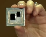
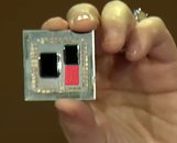
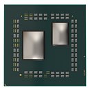
On close inspection of the substrate, we find that while the I/O controller die is somewhat centrally to the side of the package, the sole 8-core CPU chiplet is not located at a similar position (think Intel "Clarkdale" MCMs). On zooming in further, we find that just south of the 8-core CPU chiplet die, there appear to be blank bumps protruding over an area similar to that of a chiplet covered up by the outer layers of the substrate, leading us to conclude that the AM4 package is capable of three dies, an I/O controller, and two 8-core CPU chiplets. There very much will be a 16-core/32-thread Ryzen for the AM4 platform, and it's only a question of when.
The 16-core Ryzen AM4 MCM will be similar in concept to the larger 64-core SP3r2 EPYC/Threadripper MCMs: the CPU dies only pack the CPU cores and an InfinityFabric interface, while the I/O controller die is wired to multiple CPU dies, and manages the memory, PCIe, and SoC connectivity of the processor.
Interestingly, in the client-segment Intel dabbled with this concept a decade ago with "Clarkdale," which combined a 32 nm dual-core CPU die that spoke to a larger 65 nm die that controlled PCIe, memory, and an iGPU, with QPI serving as the interconnect between the two. Intel's requirements at the time were different. The company hadn't yet managed to put CPU and iGPU into a single die, and needed the iGPU to sit closer to the memory interface. The company would go onto fuse CPU and iGPU with the 32 nm "Sandy Bridge."
AMD's engineering bravado with "Matisse" also unlocks the possibility of the Ryzen "Raven Ridge" APU successor being an MCM with one 8-core chiplet, and an oversized I/O controller die that packs a "Vega" or "Navi" based iGPU, in addition to memory, PCIe, SoC, and the works. Dies on that package could be arranged differently from this.
View at TechPowerUp Main Site
This confirms that AMD is taking the heterogeneous multi-chip module approach to building its 3rd generation Ryzen processors, much like its 2nd generation EPYC processors that were unveiled late last year. The MCM of the processor Dr. Su held up had two chips, the smaller chip is an 8-core CPU chiplet built on the 7 nm process, that appears to have the same die-size as the 8-core chiplets that make up the 64-core 2nd gen EPYC MCMs, the larger die is an I/O controller logic built on the 14 nm process. This die controls the memory, PCIe, and SoC connectivity of the package. We noticed something curious about the way the two dies are arranged on the package substrate.


On close inspection of the substrate, we find that while the I/O controller die is somewhat centrally to the side of the package, the sole 8-core CPU chiplet is not located at a similar position (think Intel "Clarkdale" MCMs). On zooming in further, we find that just south of the 8-core CPU chiplet die, there appear to be blank bumps protruding over an area similar to that of a chiplet covered up by the outer layers of the substrate, leading us to conclude that the AM4 package is capable of three dies, an I/O controller, and two 8-core CPU chiplets. There very much will be a 16-core/32-thread Ryzen for the AM4 platform, and it's only a question of when.
The 16-core Ryzen AM4 MCM will be similar in concept to the larger 64-core SP3r2 EPYC/Threadripper MCMs: the CPU dies only pack the CPU cores and an InfinityFabric interface, while the I/O controller die is wired to multiple CPU dies, and manages the memory, PCIe, and SoC connectivity of the processor.
Interestingly, in the client-segment Intel dabbled with this concept a decade ago with "Clarkdale," which combined a 32 nm dual-core CPU die that spoke to a larger 65 nm die that controlled PCIe, memory, and an iGPU, with QPI serving as the interconnect between the two. Intel's requirements at the time were different. The company hadn't yet managed to put CPU and iGPU into a single die, and needed the iGPU to sit closer to the memory interface. The company would go onto fuse CPU and iGPU with the 32 nm "Sandy Bridge."
AMD's engineering bravado with "Matisse" also unlocks the possibility of the Ryzen "Raven Ridge" APU successor being an MCM with one 8-core chiplet, and an oversized I/O controller die that packs a "Vega" or "Navi" based iGPU, in addition to memory, PCIe, SoC, and the works. Dies on that package could be arranged differently from this.
View at TechPowerUp Main Site


