- Joined
- Oct 9, 2007
- Messages
- 47,878 (7.38/day)
- Location
- Dublin, Ireland
| System Name | RBMK-1000 |
|---|---|
| Processor | AMD Ryzen 7 5700G |
| Motherboard | Gigabyte B550 AORUS Elite V2 |
| Cooling | DeepCool Gammax L240 V2 |
| Memory | 2x 16GB DDR4-3200 |
| Video Card(s) | Galax RTX 4070 Ti EX |
| Storage | Samsung 990 1TB |
| Display(s) | BenQ 1440p 60 Hz 27-inch |
| Case | Corsair Carbide 100R |
| Audio Device(s) | ASUS SupremeFX S1220A |
| Power Supply | Cooler Master MWE Gold 650W |
| Mouse | ASUS ROG Strix Impact |
| Keyboard | Gamdias Hermes E2 |
| Software | Windows 11 Pro |
Intel "Ice Lake" will be the company's first major processor microarchitecture since the "Skylake" (2015), which promises CPU IPC improvements. Intel has been reusing both CPU cores and graphics architecture for four processor generations, since "Skylake". Gen9 got a mid-life update to Gen9.5 with "Kaby Lake", adding new display interfaces and faster drivers. "Ice Lake" takes advantage of the new 10 nm silicon fabrication process to not just pack faster CPU cores (with increased IPC), but also the new Gen11 iGPU. Intel published a whitepaper detailing this architecture.
An illustration in the whitepaper points to the GT2 trim of Gen11. GT2 tends to be the most common variant of each Intel graphics architecture. Gen9.5 GT2, for example, is deployed across the board on 8th and 9th generation Core processors (with the exception of the "F" or "KF" SKUs). The illustration confirms that Intel will continue to use their Ring Bus interconnect on the mainstream implementation of "Ice Lake" processors, despite possible increases in CPU core counts. This is slightly surprising, since Intel introduced a Mesh interconnect with its recent HEDT and enterprise processors. Intel has, however, ensured the iGPU has a preferential access to the Ring Bus, with 64 Byte/clock reads and 64 Byte/clock writes, while each CPU core only has 32 Byte/clock reads and 32 Byte/clock writes.
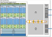
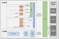
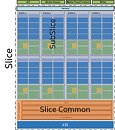

While the CPU core ring-stop terminates at its dedicated L2 cache, for the iGPU, it does so at a component called "GTI", short for graphics technology interface. The GTI interfaces with two components: Slice Common and a L3 cache which is completely separate from the processor's main L3 cache. The iGPU now has a dedicated 3 MB L3 cache, although the processor's main L3 cache outside the iGPU is still town-square for the entire processor. The iGPU's L3 cache cushions transfers between the GTI and Subslices. These are the indivisible number-crunching clusters of the GPU, much like streaming multiprocessors on an NVIDIA GPU - this is where the shaders are located. In addition to the subslices we find separate geometry processing hardware, and front-ends, including fixed-function hardware to accelerate media, which all feed into the eight subslices. The back-end is handled by "Slice Common", which includes ROPs, which write to the iGPU's own L3 cache.
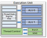
Each Subslice begins with an instruction cache and thread dispatch that divides the number-crunching workload between eight execution units or EUs. Gen11 GT2 has 64 EUs, which is a 166% growth over the 24 EUs that we saw with Gen9.5 GT2 (for example on Core i9-9900K). Such a significant increase in EUs will probably double performance, to make up lost ground against AMD's Ryzen APUs. Each EU packs two ALUs with four execution pipelines each, register files, and a thread control unit. Certain other components are shared between the EUs, such as media samplers. Intel is updating the media engine of its integrated graphics to support hardware acceleration of more video formats, including 10-bpc VP9. The display controller now supports Panel Self Refresh, Display Context Save and Restore, VESA Adaptive-Sync, and support for USB-C based outputs.
View at TechPowerUp Main Site
An illustration in the whitepaper points to the GT2 trim of Gen11. GT2 tends to be the most common variant of each Intel graphics architecture. Gen9.5 GT2, for example, is deployed across the board on 8th and 9th generation Core processors (with the exception of the "F" or "KF" SKUs). The illustration confirms that Intel will continue to use their Ring Bus interconnect on the mainstream implementation of "Ice Lake" processors, despite possible increases in CPU core counts. This is slightly surprising, since Intel introduced a Mesh interconnect with its recent HEDT and enterprise processors. Intel has, however, ensured the iGPU has a preferential access to the Ring Bus, with 64 Byte/clock reads and 64 Byte/clock writes, while each CPU core only has 32 Byte/clock reads and 32 Byte/clock writes.


While the CPU core ring-stop terminates at its dedicated L2 cache, for the iGPU, it does so at a component called "GTI", short for graphics technology interface. The GTI interfaces with two components: Slice Common and a L3 cache which is completely separate from the processor's main L3 cache. The iGPU now has a dedicated 3 MB L3 cache, although the processor's main L3 cache outside the iGPU is still town-square for the entire processor. The iGPU's L3 cache cushions transfers between the GTI and Subslices. These are the indivisible number-crunching clusters of the GPU, much like streaming multiprocessors on an NVIDIA GPU - this is where the shaders are located. In addition to the subslices we find separate geometry processing hardware, and front-ends, including fixed-function hardware to accelerate media, which all feed into the eight subslices. The back-end is handled by "Slice Common", which includes ROPs, which write to the iGPU's own L3 cache.
Each Subslice begins with an instruction cache and thread dispatch that divides the number-crunching workload between eight execution units or EUs. Gen11 GT2 has 64 EUs, which is a 166% growth over the 24 EUs that we saw with Gen9.5 GT2 (for example on Core i9-9900K). Such a significant increase in EUs will probably double performance, to make up lost ground against AMD's Ryzen APUs. Each EU packs two ALUs with four execution pipelines each, register files, and a thread control unit. Certain other components are shared between the EUs, such as media samplers. Intel is updating the media engine of its integrated graphics to support hardware acceleration of more video formats, including 10-bpc VP9. The display controller now supports Panel Self Refresh, Display Context Save and Restore, VESA Adaptive-Sync, and support for USB-C based outputs.
View at TechPowerUp Main Site


