- Joined
- Oct 9, 2007
- Messages
- 47,572 (7.46/day)
- Location
- Dublin, Ireland
| System Name | RBMK-1000 |
|---|---|
| Processor | AMD Ryzen 7 5700G |
| Motherboard | ASUS ROG Strix B450-E Gaming |
| Cooling | DeepCool Gammax L240 V2 |
| Memory | 2x 8GB G.Skill Sniper X |
| Video Card(s) | Palit GeForce RTX 2080 SUPER GameRock |
| Storage | Western Digital Black NVMe 512GB |
| Display(s) | BenQ 1440p 60 Hz 27-inch |
| Case | Corsair Carbide 100R |
| Audio Device(s) | ASUS SupremeFX S1220A |
| Power Supply | Cooler Master MWE Gold 650W |
| Mouse | ASUS ROG Strix Impact |
| Keyboard | Gamdias Hermes E2 |
| Software | Windows 11 Pro |
AMD will launch its 3rd generation Ryzen 3000 Socket AM4 desktop processors in 2019, with a product unveiling expected mid-year, likely on the sidelines of Computex 2019. AMD is keeping its promise of making these chips backwards compatible with existing Socket AM4 motherboards. To that effect, motherboard vendors such as ASUS and MSI began rolling out BIOS updates with AGESA-Combo 0.0.7.x microcode, which adds initial support for the platform to run and validate engineering samples of the upcoming "Zen 2" chips.
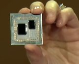
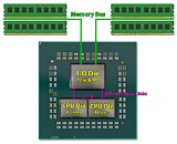
At CES 2019, AMD unveiled more technical details and a prototype of a 3rd generation Ryzen socket AM4 processor. The company confirmed that it will implement a multi-chip module (MCM) design even for their mainstream-desktop processor, in which it will use one or two 7 nm "Zen 2" CPU core chiplets, which talk to a 14 nm I/O controller die over Infinity Fabric. The two biggest components of the IO die are the PCI-Express root complex, and the all-important dual-channel DDR4 memory controller. We bring you never before reported details of this memory controller.

AMD has two big reasons to take the MCM route for even its mainstream desktop platform. The first is that it lets them mix-and-match silicon production technologies. AMD bean-counters reckon that it's more economical to build only those components on a shrunk 7 nanometer production process, which can benefit from the shrink; namely the CPU cores. Other components like the memory controller can continue to be built on existing 14 nm technologies, which by now are highly mature (= cost-efficient). AMD is also competing with other companies for its share of 7 nanometer allocation at TSMC.
The 14 nm I/O controller die could, in theory, be sourced from GlobalFoundries to honor the wafer-supply agreement. The second big reason is the economics of downscaling. AMD is expected to increase CPU core counts beyond 8 and cramming 12-16 cores on a single 7 nm slab will make carving out cheaper SKUs by disabling cores costly, because AMD isn't always harvesting dies with faulty cores. These mid-range SKUs sell in higher volumes, and beyond a point AMD is forced to disable perfectly functional cores. It makes more sense to build 8-core or 6-core chiplets, and on SKUs with 8 cores or fewer, physically deploy only one chiplet. This way AMD is maximizing its utilization of precious 7 nm wafers.

The downside of this approach is the memory controller is no longer physically integrated with the processor cores. The 3rd generation Ryzen processor (and all other Zen 2 CPUs), hence have an "integrated-discrete" memory controller. The memory controller is physically located inside the processor, but is not on the same piece of silicon as the CPU cores. AMD isn't the first to come up with such a contraption. Intel's 1st generation Core "Clarkdale" processor took a similar route, with CPU cores on a 32 nm die, and the memory controller plus an integrated GPU on a separate 45 nm die.
Intel used its Quick Path Interconnect (QPI), which was cutting-edge at the time. AMD is tapping into Infinity Fabric, its latest high-bandwidth scalable interconnect that's heavily implemented on "Zen" and "Vega" product lines. We have learned that with "Matisse," AMD will be introducing a new version of Infinity Fabric that offers twice the bandwidth compared to the first generation, or up to 100 GB/s. AMD needs this because a single I/O controller die must now interface with up to two 8-core CPU dies, and up to 64 cores in their "EPYC" server line SKU.
Our resident Ryzen Memory Guru Yuri "1usmus" Bubliy took a really close look at one of these BIOS updates with AGESA 0.0.7.x and found several new controls and options that will be exclusive to "Matisse," and possibly the next-generation Ryzen Threadripper processors. AMD has changed the CBS section title from "Zen Common Options" to "Valhalla Common Options." We have seen this codename on the web quite a bit over the past few days, associated with "Zen 2." We have learned that "Valhalla" could be the codename of the platform consisting of a 3rd generation Ryzen "Matisse" AM4 processor and its companion AMD 500-series chipset based motherboard, specifically the successor to X470 which is being developed in-house by AMD as opposed to sourcing from ASMedia.
When doing serious memory overclocking, it can happen that the Infinity Fabric can't handle the increased memory speed. Remember, Infinity Fabric runs at a frequency synchronized to memory. For example, with DDR-3200 memory (which runs at 1600 MHz), Infinity Fabric will operate at 1600 MHz. This is the default of Zen, Zen+ and also Zen 2. Unlike earlier generations, the new BIOS offers UCLK options for "Auto", "UCLK==MEMCLK" and "UCLK==MEMCLK/2". The last option is new and will come in handy when overclocking your memory, to achieve stability, but at the cost of some Infinity Fabric bandwidth.
Precision Boost Overdrive will receive more fine-grained control at the BIOS level, and AMD is making significant changes to this feature to make the boost setting more flexible and improve the algorithm. Early adopters of AGESA Combo 0.0.7.x on AMD 400-series chipset motherboards noticed that PBO broke or became buggy on their machines. This is because of poor integration of the new PBO algorithm with the existing one compatible with "Pinnacle Ridge." AMD also implemented "Core Watchdog", a feature that resets the system in case address or data errors destabilize the machine.
The "Matisse" processor will also provide users with finer control over active cores. Since the AM4 package has two 8-core chiplets, you will have the option to disable an entire chiplet, or adjust the core-count in decrements of 2, since each 8-core chiplet consists of two 4-core CCX (compute complexes), much like existing AMD designs. At the chiplet-level you can dial down core counts from 4+4 to 3+3, 2+2, and 1+1, but never asymmetrically, such as 4+0 (which was possible on first-generation Zen). AMD is synchronizing CCX core counts for optimal utilization of L3 cache and memory access. For the 64-core Threadripper that has eight 8-core chiplets, you will be able to disable chiplets as long as you have at least two chiplets enabled.
CAKE, or "coherent AMD socket extender" received an additional setting, namely "CAKE CRC performance Bounds". AMD is implementing IFOP (Infinity Fabric On Package,) or the non-socketed version of IF, in three places on the "Matisse" MCM. The I/O controller die has 100 GB/s IFOP links to each of the two 8-core chiplets, and another 100 GB/s IFOP link connects the two chiplets to each other. For multi-socket implementations of "Zen 2," AMD will provide NUMA node controls, namely "NUMA nodes per socket," with options including "NPS0", "NPS1", "NPS2", "NPS4" and "Auto".
With "Zen 2," AMD is introducing a couple of major new DCT-level features. The first one is called "DRAM Map Inversion," with options including "Disabled", "Enabled" and "Auto". The motherboard vendor description of this option goes like "Properly utilize the parallelism within a channel and DRAM device. Bits that flip more frequently should be used to map resources of greater parallelism within the system." Another is "DRAM Post Package Repair," with options including "Enabled", "Disabled", and "Auto." This new special mode (which is a JEDEC standard) lets the memory manufacturer increase DRAM yields by selectively disabling bad memory cells, to replace them automatically with working ones from a spare area, similar to how storage devices map out bad sectors. We're not sure why such a feature is being exposed to end-users, especially from the client-segment. Perhaps it will be removed on production motherboards.
We've also come across an interesting option related to the I/O controller that lets you select PCI-Express generation up to "Gen 4.0". This could indicate some existing 400-series chipset motherboards could receive PCI-Express Gen 4.0, given that we're examining a 400-series chipset motherboard's firmware. We've heard through credible sources that AMD's PCIe Gen 4.0 implementation involves the use of external re-driver devices on the motherboard. These don't come cheap. Texas Instruments sells Gen 3.0 redrivers for $1.5 a piece in 1,000-unit reel quantities. Motherboard vendors will have to fork out quite at least $15-20 on socket AM4 motherboards with Gen 4.0 slots, given that you need 20 of these redrivers, one per lane. We've come across several other common controls, including "RCD Parity" and "Memory MBIST" (a new memory self-test program).
One of the firmware setup program pages is titled "SoC Miscellaneous Control," and includes the following settings, many of which are industry-standard:
All in all, AMD Ryzen "Matisse" promises to give advanced and enthusiast users a treasure-chest of tuning options. Thanks again to Yuri "1usmus" Bubliy, who contributed significantly to this article.
View at TechPowerUp Main Site
At CES 2019, AMD unveiled more technical details and a prototype of a 3rd generation Ryzen socket AM4 processor. The company confirmed that it will implement a multi-chip module (MCM) design even for their mainstream-desktop processor, in which it will use one or two 7 nm "Zen 2" CPU core chiplets, which talk to a 14 nm I/O controller die over Infinity Fabric. The two biggest components of the IO die are the PCI-Express root complex, and the all-important dual-channel DDR4 memory controller. We bring you never before reported details of this memory controller.

AMD has two big reasons to take the MCM route for even its mainstream desktop platform. The first is that it lets them mix-and-match silicon production technologies. AMD bean-counters reckon that it's more economical to build only those components on a shrunk 7 nanometer production process, which can benefit from the shrink; namely the CPU cores. Other components like the memory controller can continue to be built on existing 14 nm technologies, which by now are highly mature (= cost-efficient). AMD is also competing with other companies for its share of 7 nanometer allocation at TSMC.
The 14 nm I/O controller die could, in theory, be sourced from GlobalFoundries to honor the wafer-supply agreement. The second big reason is the economics of downscaling. AMD is expected to increase CPU core counts beyond 8 and cramming 12-16 cores on a single 7 nm slab will make carving out cheaper SKUs by disabling cores costly, because AMD isn't always harvesting dies with faulty cores. These mid-range SKUs sell in higher volumes, and beyond a point AMD is forced to disable perfectly functional cores. It makes more sense to build 8-core or 6-core chiplets, and on SKUs with 8 cores or fewer, physically deploy only one chiplet. This way AMD is maximizing its utilization of precious 7 nm wafers.

The downside of this approach is the memory controller is no longer physically integrated with the processor cores. The 3rd generation Ryzen processor (and all other Zen 2 CPUs), hence have an "integrated-discrete" memory controller. The memory controller is physically located inside the processor, but is not on the same piece of silicon as the CPU cores. AMD isn't the first to come up with such a contraption. Intel's 1st generation Core "Clarkdale" processor took a similar route, with CPU cores on a 32 nm die, and the memory controller plus an integrated GPU on a separate 45 nm die.
Intel used its Quick Path Interconnect (QPI), which was cutting-edge at the time. AMD is tapping into Infinity Fabric, its latest high-bandwidth scalable interconnect that's heavily implemented on "Zen" and "Vega" product lines. We have learned that with "Matisse," AMD will be introducing a new version of Infinity Fabric that offers twice the bandwidth compared to the first generation, or up to 100 GB/s. AMD needs this because a single I/O controller die must now interface with up to two 8-core CPU dies, and up to 64 cores in their "EPYC" server line SKU.
Our resident Ryzen Memory Guru Yuri "1usmus" Bubliy took a really close look at one of these BIOS updates with AGESA 0.0.7.x and found several new controls and options that will be exclusive to "Matisse," and possibly the next-generation Ryzen Threadripper processors. AMD has changed the CBS section title from "Zen Common Options" to "Valhalla Common Options." We have seen this codename on the web quite a bit over the past few days, associated with "Zen 2." We have learned that "Valhalla" could be the codename of the platform consisting of a 3rd generation Ryzen "Matisse" AM4 processor and its companion AMD 500-series chipset based motherboard, specifically the successor to X470 which is being developed in-house by AMD as opposed to sourcing from ASMedia.
When doing serious memory overclocking, it can happen that the Infinity Fabric can't handle the increased memory speed. Remember, Infinity Fabric runs at a frequency synchronized to memory. For example, with DDR-3200 memory (which runs at 1600 MHz), Infinity Fabric will operate at 1600 MHz. This is the default of Zen, Zen+ and also Zen 2. Unlike earlier generations, the new BIOS offers UCLK options for "Auto", "UCLK==MEMCLK" and "UCLK==MEMCLK/2". The last option is new and will come in handy when overclocking your memory, to achieve stability, but at the cost of some Infinity Fabric bandwidth.
Precision Boost Overdrive will receive more fine-grained control at the BIOS level, and AMD is making significant changes to this feature to make the boost setting more flexible and improve the algorithm. Early adopters of AGESA Combo 0.0.7.x on AMD 400-series chipset motherboards noticed that PBO broke or became buggy on their machines. This is because of poor integration of the new PBO algorithm with the existing one compatible with "Pinnacle Ridge." AMD also implemented "Core Watchdog", a feature that resets the system in case address or data errors destabilize the machine.
The "Matisse" processor will also provide users with finer control over active cores. Since the AM4 package has two 8-core chiplets, you will have the option to disable an entire chiplet, or adjust the core-count in decrements of 2, since each 8-core chiplet consists of two 4-core CCX (compute complexes), much like existing AMD designs. At the chiplet-level you can dial down core counts from 4+4 to 3+3, 2+2, and 1+1, but never asymmetrically, such as 4+0 (which was possible on first-generation Zen). AMD is synchronizing CCX core counts for optimal utilization of L3 cache and memory access. For the 64-core Threadripper that has eight 8-core chiplets, you will be able to disable chiplets as long as you have at least two chiplets enabled.
CAKE, or "coherent AMD socket extender" received an additional setting, namely "CAKE CRC performance Bounds". AMD is implementing IFOP (Infinity Fabric On Package,) or the non-socketed version of IF, in three places on the "Matisse" MCM. The I/O controller die has 100 GB/s IFOP links to each of the two 8-core chiplets, and another 100 GB/s IFOP link connects the two chiplets to each other. For multi-socket implementations of "Zen 2," AMD will provide NUMA node controls, namely "NUMA nodes per socket," with options including "NPS0", "NPS1", "NPS2", "NPS4" and "Auto".
With "Zen 2," AMD is introducing a couple of major new DCT-level features. The first one is called "DRAM Map Inversion," with options including "Disabled", "Enabled" and "Auto". The motherboard vendor description of this option goes like "Properly utilize the parallelism within a channel and DRAM device. Bits that flip more frequently should be used to map resources of greater parallelism within the system." Another is "DRAM Post Package Repair," with options including "Enabled", "Disabled", and "Auto." This new special mode (which is a JEDEC standard) lets the memory manufacturer increase DRAM yields by selectively disabling bad memory cells, to replace them automatically with working ones from a spare area, similar to how storage devices map out bad sectors. We're not sure why such a feature is being exposed to end-users, especially from the client-segment. Perhaps it will be removed on production motherboards.
We've also come across an interesting option related to the I/O controller that lets you select PCI-Express generation up to "Gen 4.0". This could indicate some existing 400-series chipset motherboards could receive PCI-Express Gen 4.0, given that we're examining a 400-series chipset motherboard's firmware. We've heard through credible sources that AMD's PCIe Gen 4.0 implementation involves the use of external re-driver devices on the motherboard. These don't come cheap. Texas Instruments sells Gen 3.0 redrivers for $1.5 a piece in 1,000-unit reel quantities. Motherboard vendors will have to fork out quite at least $15-20 on socket AM4 motherboards with Gen 4.0 slots, given that you need 20 of these redrivers, one per lane. We've come across several other common controls, including "RCD Parity" and "Memory MBIST" (a new memory self-test program).
One of the firmware setup program pages is titled "SoC Miscellaneous Control," and includes the following settings, many of which are industry-standard:
- DRAM Address Command Parity Retry
- Max Parity Error Replay
- Write CRC Enable
- DRAM Write CRC Enable and Retry Limit
- Max Write CRC Error Replay
- Disable Memory Error Injection
- DRAM UECC Retry
- ACPI Settings:
o ACPI SRAT L3 Cache As NUMA Domain
o ACPI SLIT Distance Control
o ACPI SLIT remote relative distance
o ACPI SLIT virtual distance
o ACPI SLIT same socket distance
o ACPI SLIT remote socket distance
o ACPI SLIT local SLink distance
o ACPI SLIT remote SLink distance
o ACPI SLIT local inter-SLink distance
o ACPI SLIT remote inter-SLink distance - CLDO_VDDP Control
- Efficiency Mode
- Package Power Limit Control
- DF C-states
- Fixed SOC P-state
- CPPC
- 4-link xGMI max speed
- 3-link xGMI max speed
All in all, AMD Ryzen "Matisse" promises to give advanced and enthusiast users a treasure-chest of tuning options. Thanks again to Yuri "1usmus" Bubliy, who contributed significantly to this article.
View at TechPowerUp Main Site


