Raevenlord
News Editor
- Joined
- Aug 12, 2016
- Messages
- 3,755 (1.20/day)
- Location
- Portugal
| System Name | The Ryzening |
|---|---|
| Processor | AMD Ryzen 9 5900X |
| Motherboard | MSI X570 MAG TOMAHAWK |
| Cooling | Lian Li Galahad 360mm AIO |
| Memory | 32 GB G.Skill Trident Z F4-3733 (4x 8 GB) |
| Video Card(s) | Gigabyte RTX 3070 Ti |
| Storage | Boot: Transcend MTE220S 2TB, Kintson A2000 1TB, Seagate Firewolf Pro 14 TB |
| Display(s) | Acer Nitro VG270UP (1440p 144 Hz IPS) |
| Case | Lian Li O11DX Dynamic White |
| Audio Device(s) | iFi Audio Zen DAC |
| Power Supply | Seasonic Focus+ 750 W |
| Mouse | Cooler Master Masterkeys Lite L |
| Keyboard | Cooler Master Masterkeys Lite L |
| Software | Windows 10 x64 |
Public perception on NVIDIA's new RTX series of graphics cards was sometimes marred by an impression of wrong resource allocation from NVIDIA. The argument went that NVIDIA had greatly increased chip area by adding RTX functionality (in both its Tensor ad RT cores) that could have been better used for increased performance gains in shader-based, non-raytracing workloads. While the merits of ray tracing oas it stands (in terms of uptake from developers) are certainly worthy of discussion, it seems that NVIDIA didn't dedicate that much more die area to their RTX functionality - at least not to the tone of public perception.
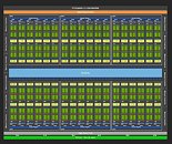
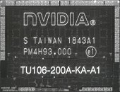
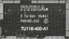
After analyzing full, high-res images of NVIDIA's TU106 and TU116 chips, reddit user @Qesa did some analysis on the TPC structure of NVIDIA's Turing chips, and arrived at the conclusion that the difference between NVIDIA's RTX-capable TU106 compared to their RTX-stripped TU116 amounts to a mere 1.95 mm² of additional logic per TPC - a 22% area increase. Of these, 1.25 mm² are reserved for the Tensor logic (which accelerates both DLSS and de-noising on ray-traced workloads), while only 0.7 mm² are being used for the RT cores.
According to the math, this means that a TU102 chip used for the RTX 2080 Ti, which in its full configuration, has a 754 mm² area, could have done with a 684 mm² chip instead. It seems that most of the area increase compared to the Pascal architecture actually comes from increased performance (and size) of caches and larger instruction sets on Turing than from RTX functionality. Not accounting to area density achieved from the transition from 16 nm to 12 nm, a TU106 chip powering an RTX 2060 delivers around the same performance as the GP104 chip powering the GTX 1080 (410 mm² on the TU106 against 314 mm² on GP104), whilst carrying only 75% of the SM count (1920 versus 2560 SMs).
View at TechPowerUp Main Site
After analyzing full, high-res images of NVIDIA's TU106 and TU116 chips, reddit user @Qesa did some analysis on the TPC structure of NVIDIA's Turing chips, and arrived at the conclusion that the difference between NVIDIA's RTX-capable TU106 compared to their RTX-stripped TU116 amounts to a mere 1.95 mm² of additional logic per TPC - a 22% area increase. Of these, 1.25 mm² are reserved for the Tensor logic (which accelerates both DLSS and de-noising on ray-traced workloads), while only 0.7 mm² are being used for the RT cores.


According to the math, this means that a TU102 chip used for the RTX 2080 Ti, which in its full configuration, has a 754 mm² area, could have done with a 684 mm² chip instead. It seems that most of the area increase compared to the Pascal architecture actually comes from increased performance (and size) of caches and larger instruction sets on Turing than from RTX functionality. Not accounting to area density achieved from the transition from 16 nm to 12 nm, a TU106 chip powering an RTX 2060 delivers around the same performance as the GP104 chip powering the GTX 1080 (410 mm² on the TU106 against 314 mm² on GP104), whilst carrying only 75% of the SM count (1920 versus 2560 SMs).
View at TechPowerUp Main Site


