- Joined
- Oct 9, 2007
- Messages
- 47,230 (7.55/day)
- Location
- Hyderabad, India
| System Name | RBMK-1000 |
|---|---|
| Processor | AMD Ryzen 7 5700G |
| Motherboard | ASUS ROG Strix B450-E Gaming |
| Cooling | DeepCool Gammax L240 V2 |
| Memory | 2x 8GB G.Skill Sniper X |
| Video Card(s) | Palit GeForce RTX 2080 SUPER GameRock |
| Storage | Western Digital Black NVMe 512GB |
| Display(s) | BenQ 1440p 60 Hz 27-inch |
| Case | Corsair Carbide 100R |
| Audio Device(s) | ASUS SupremeFX S1220A |
| Power Supply | Cooler Master MWE Gold 650W |
| Mouse | ASUS ROG Strix Impact |
| Keyboard | Gamdias Hermes E2 |
| Software | Windows 11 Pro |
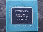
During our disassembly of the GeForce RTX 2060 Super, we noticed a shocking detail. The 12 nm "TU106" GPU on which it is based, has the marking "Korea." We know for a fact that TSMC does not have any fabs there. The only Korean semiconductor manufacturer capable of contract-manufacturing a piece of silicon as complex as a GPU, for a designer with the energy-efficiency OCD as NVIDIA, is Samsung.
What makes this interesting is that Samsung does not officially have a 12 nm FinFET process. It has 14 nm, and the 11LPP, a 11 nm nodelet, which the company designed to compete with TSMC 12 nm. It would hence be really interesting to hear from NVIDIA on whether they've scaled out the "TU106" to 14LPP, or down to 11LPP at Samsung. It's interesting to note that the shrink in transistor sizes in these nodelets doesn't affect die-sizes. We hence see no die-size difference between these Korea-marked chips, and those marked "Taiwan." We've reached out to NVIDIA for comment.
Update July 3rd: NVIDIA got back to us

View at TechPowerUp Main Site
What makes this interesting is that Samsung does not officially have a 12 nm FinFET process. It has 14 nm, and the 11LPP, a 11 nm nodelet, which the company designed to compete with TSMC 12 nm. It would hence be really interesting to hear from NVIDIA on whether they've scaled out the "TU106" to 14LPP, or down to 11LPP at Samsung. It's interesting to note that the shrink in transistor sizes in these nodelets doesn't affect die-sizes. We hence see no die-size difference between these Korea-marked chips, and those marked "Taiwan." We've reached out to NVIDIA for comment.
Update July 3rd: NVIDIA got back to us
NVIDIA said:The answer is really simple and these markings are not new. Other Turing GPUs have had these markings in the past. The chip is made at TSMC, but packaged in various locations. This one was done in Korea, hence why his says "Korea".
On an unrelated note: We already use both TSMC and Samsung, and qualify each of them for every process node. We can't comment in any further detail on future plans, but both remain terrific partners.

View at TechPowerUp Main Site


