• Welcome to TechPowerUp Forums, Guest! Please check out our forum guidelines for info related to our community.
  • The forums have been upgraded with support for dark mode. By default it will follow the setting on your system/browser. You may override it by scrolling to the end of the page and clicking the gears icon.

AMD Sheds Light on the Missing "+" in "7nm" for Zen 3 and RDNA2 in its Latest Presentation

btarunr

Editor & Senior Moderator
Staff member
Joined
Oct 9, 2007
Messages
47,849 (7.39/day)
Location
Dublin, Ireland
System Name RBMK-1000
Processor AMD Ryzen 7 5700G
Motherboard Gigabyte B550 AORUS Elite V2
Cooling DeepCool Gammax L240 V2
Memory 2x 16GB DDR4-3200
Video Card(s) Galax RTX 4070 Ti EX
Storage Samsung 990 1TB
Display(s) BenQ 1440p 60 Hz 27-inch
Case Corsair Carbide 100R
Audio Device(s) ASUS SupremeFX S1220A
Power Supply Cooler Master MWE Gold 650W
Mouse ASUS ROG Strix Impact
Keyboard Gamdias Hermes E2
Software Windows 11 Pro
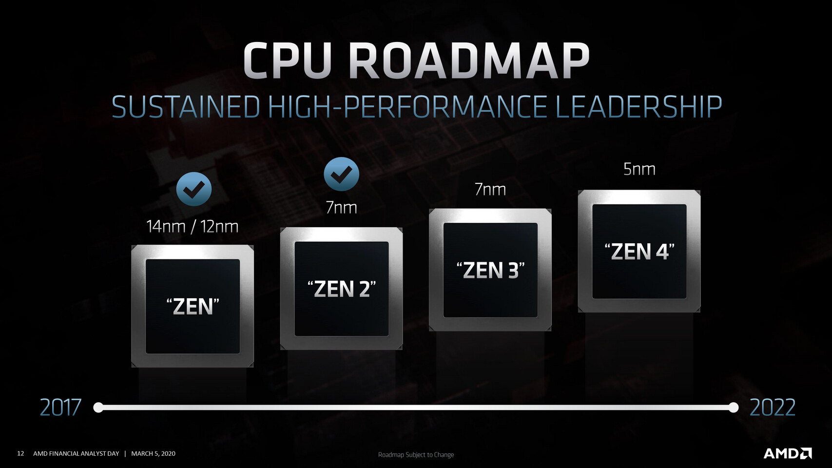
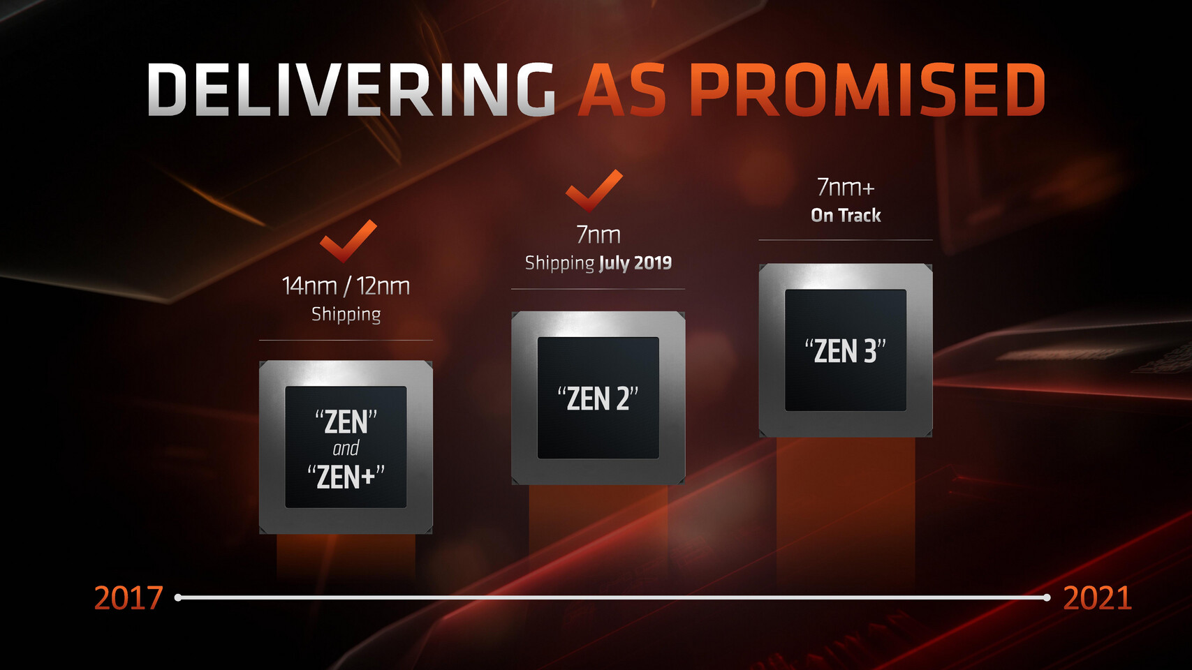
AMD at its Financial Analyst Day 2020 presentation made a major clarification about its silicon fabrication process. It was previously believed that the company's upcoming "Zen 3" CPU microarchitecture and RDNA2 graphics architectures were based on TSMC's N7+ (7 nm EUV) silicon fabrication process because AMD would mark the two as "7 nm+" in its marketing slides. Throughout its Financial Analyst Day presentation, however, AMD avoided using that marker, and resorted to an amorphous "7 nm" marker, prompting one of the financial analysts to seek a clarification. At the time, AMD responded that they were aligning their marketing with that of TSMC, and hence chose to use "7 nm" in its new slides.

It turns out that the next step to TSMC N7, the company's current-generation 7 nm DUV silicon fabrication node, isn't N7+ (7 nm EUV), but rather it has a nodelet along the way, which the foundry refers to as N7P. This is a generational refinement of N7, but does not use EUV lithography, which means it may not offer the 15-20 percent gains in transistor densities offered by N7+ over N7. AMD clarified that "7 nm+" in its past presentations did not intend to signify N7+, and that the "+" merely denoted an improvement over N7. At the same time, it won't specify whether "Zen 3" and RDNA2 are based on N7P or N7+, so the company doesn't rule out N7+, either. We'll probably learn more as we near the late-2020 launch of "Zen 3" as EPYC "Milan."


View at TechPowerUp Main Site
 
N7 vs N7P
+7% Perf. or -10% Power

N7 vs N7+
+10% Perf. or -15% Power
1-1260.jpg

N7P

TSMC has started rolling out an optimized version of their N7 process called N7 Performance-enhanced version (N7P). This process goes by various other names such as “2nd generation 7 nm” and “7 nm year 2”. This process should not be confused with N7+. N7P is an optimized, DUV-based, process which uses the same design rules and is fully IP-compatible with N7. N7P introduces FEOL and MOL optimizations which are said to translate to either 7% performance improvement at iso-power or up to 10% lower power at iso-speed.

N7+

TSMC’s N7+ is their first process technology to adopt EUV for a few critical layers. N7+ entered mass production last quarter (Q2). TSMC says they have demonstrated similar yield to N7. Compared to their N7 process, N7+ is said to deliver around 1.2x density improvement. N7+ is said to deliver 10% higher performance at iso-power or, alternatively, up to 15% lower power at iso-performance. On paper, N7+ appears to be marginally better than N7P. Though keep in mind that those improvements can only be obtained through a new physical re-implementation and new EUV masks.
 
Last edited:
2030 7nm++++++++++++

Intel stuck with 14nm, AMD 7nm. o_O
 
On paper, N7+ appears to be marginally better than N7P. Though keep in mind that those improvements can only be obtained through a new physical re-implementation and new EUV masks.
Cost savings in optical masks sounds pretty good.
 
Cost savings in optical masks sounds pretty good.
Yeah, especially when no Zen3+ steps are required with getting an early N5 with Zen4 in 2021.
 
I just hope RDNA2 is somewhat competitive against Nvidia so they can give us more cuda cores, which is rumored to go upto 8k cores on the Tesla variant!
The relevance of your post is 0.1%

Troll much.
 
So... the headline/article that says RDNA2 will be 50% more efficient still stands?
 
Yes, best case scenario (vs the most inefficient Navi?) I'd say why not.
 
"Mark Papermaster clarified in the Q&A section afterwards. TSMC are now just including N7+ in N7 as additional libraries, AMD are just following their nomenclature now. They're still 'N7+' products in that they use EUV for some layers "

Whatever the heck that means.
 
"Mark Papermaster clarified in the Q&A section afterwards. TSMC are now just including N7+ in N7 as additional libraries, AMD are just following their nomenclature now. They're still 'N7+' products in that they use EUV for some layers "

Whatever the heck that means.
This could mean that N7P is not DUV only and eventually makes also use of EUV in some layers, but without the heavier changes to the IP wich would be necessary with N7+.
Or there is some sort of N7+-lite wich uses nearly no to none IP-breaking at all. So it would be like a mix of N7P and N7+, sort of.
 
7% ~ 300Mhz, so nice. 4.7Ghz is quite impressive. The first EUV is N6 perhaps next year.
 
"Mark Papermaster clarified in the Q&A section afterwards. TSMC are now just including N7+ in N7 as additional libraries, AMD are just following their nomenclature now. They're still 'N7+' products in that they use EUV for some layers "

Whatever the heck that means.

It means what I predicted a year or so back, these nodes are coming about much slower than they are presented to us. A full EUV 7nm will deliver a far more powerful chip.

We will be riding 7nm for several years from today, make no mistake. Its an uphill battleand every baby step has to overcome yield and cost issues.

Now you also know why neither Intel or Nvidia was eager to early adopt 7nm.
 
They are using EUV only where it is not mission critical, but saves masking layers. They will be using it on copper contacts and all.
 
no crytical layers none of that. just simple N7P or direct shrink to N6 EUV that is specifically built to use the same design rules as DUV, for 18% better density. But I dont believe that N5 will ever be used by AMD, it requires different rules and redesigns. This N7P branch ends with N6, and the story ends there. Jumping from N7 to N5 or N3 after that is very unlikely. I mean what comes next 128 core, 256?, this would be insane core count.
 
Last edited:
AnandTech has apparently missed the fact that Navi10 is already N7P, so if it's "enhanced 7nm" compared to Navi10, it should be N7+ EUV (unless TSMC has different, newer libraries for N7P)

"Mark Papermaster clarified in the Q&A section afterwards. TSMC are now just including N7+ in N7 as additional libraries, AMD are just following their nomenclature now. They're still 'N7+' products in that they use EUV for some layers "

Whatever the heck that means.

N7+ uses EUV only for some layers, it's been known since TSMC told about the process years ago
 
Back
Top