- Joined
- Aug 19, 2017
- Messages
- 2,732 (1.01/day)
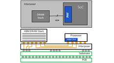
Rambus, a maker of various Interface IP solutions, today announced the latest addition to its high-speed memory interface IP product portfolio in form of High Bandwidth Memory 2E (HBM2E) controller and physical layer (PHY) IP solution. The two IPs are enabling customers to completely integrate the HBM2E memory into their products, given that Rambus provides a complete solution for controlling and interfacing the memory. The design that Ramus offers can support for 12-high DRAM stacks of up to 24 Gb devices, making for up to 36 GB of memory per 3D stack. This single 3D stack is capable of delivering 3.2 Gbps over a 1024-bit wide interface, delivering 410 GB/s of bandwidth per stack.
The HBM2E controller core is DFI 3.1 compatible and has support for logic interfaces like AXI, OCP, or a custom one, so the customer can choose a way to integrate this core in their design. With a purchase of their HBM2E IP, Rambus will provide source code written in Hardware Description Language (HDL) and GDSII file containing the layout of the interface.


View at TechPowerUp Main Site
The HBM2E controller core is DFI 3.1 compatible and has support for logic interfaces like AXI, OCP, or a custom one, so the customer can choose a way to integrate this core in their design. With a purchase of their HBM2E IP, Rambus will provide source code written in Hardware Description Language (HDL) and GDSII file containing the layout of the interface.


View at TechPowerUp Main Site


