- Joined
- Oct 9, 2007
- Messages
- 47,537 (7.47/day)
- Location
- Hyderabad, India
| System Name | RBMK-1000 |
|---|---|
| Processor | AMD Ryzen 7 5700G |
| Motherboard | ASUS ROG Strix B450-E Gaming |
| Cooling | DeepCool Gammax L240 V2 |
| Memory | 2x 8GB G.Skill Sniper X |
| Video Card(s) | Palit GeForce RTX 2080 SUPER GameRock |
| Storage | Western Digital Black NVMe 512GB |
| Display(s) | BenQ 1440p 60 Hz 27-inch |
| Case | Corsair Carbide 100R |
| Audio Device(s) | ASUS SupremeFX S1220A |
| Power Supply | Cooler Master MWE Gold 650W |
| Mouse | ASUS ROG Strix Impact |
| Keyboard | Gamdias Hermes E2 |
| Software | Windows 11 Pro |
A Forbes report provides a fascinating peek into something that could explain GlobalFoundries stalling its 7 nm-class silicon fabrication plans, and shedding much of its offshore foundry bulk, other than just fiscal prudence. Apparently, the company has been making moves in silicon photonics, benefiting from few of the 16,000+ patents and other forms of IP it inherited from the IBM Microelectronics business acquisition from 2015. In particular, GlobalFoundries appears interested in high-bandwidth networking physical-layer applications that involve photonics and fiber-optics.
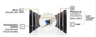
GlobalFoundries has reportedly been engaging with customers in the telecom- and data-center industries since 2016 in offering medium-range networking physical-layer solution, providing 40 Gbps bandwidths over distances of up to 10 km (without repeaters in the middle). In 2017, it partnered with Ayar Labs to develop an optical I/O chip. This solution combines Ayar's optical CMOS I/O tech with GloFo's 45 nm CMOS process to 10x the bandwidth at 1/5th the power of a copper-based I/O. By 2018, the combine qualified a platform that can push up to 100 Gbps per wavelength, and up to 800 Gbps on the client-side. By 2019, the combine developed a supercomputing chiplet co-packed with an Intel silicon as part of DARPA's PIPES (Photonics in Package for Extreme Scalability) project. With network bandwidth demand on an exponential rise with the advent of 5G, I guess you can say that the future for GloFo's silicon photonics business looks bright.


View at TechPowerUp Main Site
GlobalFoundries has reportedly been engaging with customers in the telecom- and data-center industries since 2016 in offering medium-range networking physical-layer solution, providing 40 Gbps bandwidths over distances of up to 10 km (without repeaters in the middle). In 2017, it partnered with Ayar Labs to develop an optical I/O chip. This solution combines Ayar's optical CMOS I/O tech with GloFo's 45 nm CMOS process to 10x the bandwidth at 1/5th the power of a copper-based I/O. By 2018, the combine qualified a platform that can push up to 100 Gbps per wavelength, and up to 800 Gbps on the client-side. By 2019, the combine developed a supercomputing chiplet co-packed with an Intel silicon as part of DARPA's PIPES (Photonics in Package for Extreme Scalability) project. With network bandwidth demand on an exponential rise with the advent of 5G, I guess you can say that the future for GloFo's silicon photonics business looks bright.


View at TechPowerUp Main Site

