• Welcome to TechPowerUp Forums, Guest! Please check out our forum guidelines for info related to our community.

NVIDIA "Ampere" Designed for both HPC and GeForce/Quadro

btarunr

Editor & Senior Moderator
Staff member
Joined
Oct 9, 2007
Messages
47,677 (7.43/day)
Location
Dublin, Ireland
System Name RBMK-1000
Processor AMD Ryzen 7 5700G
Motherboard Gigabyte B550 AORUS Elite V2
Cooling DeepCool Gammax L240 V2
Memory 2x 16GB DDR4-3200
Video Card(s) Galax RTX 4070 Ti EX
Storage Samsung 990 1TB
Display(s) BenQ 1440p 60 Hz 27-inch
Case Corsair Carbide 100R
Audio Device(s) ASUS SupremeFX S1220A
Power Supply Cooler Master MWE Gold 650W
Mouse ASUS ROG Strix Impact
Keyboard Gamdias Hermes E2
Software Windows 11 Pro
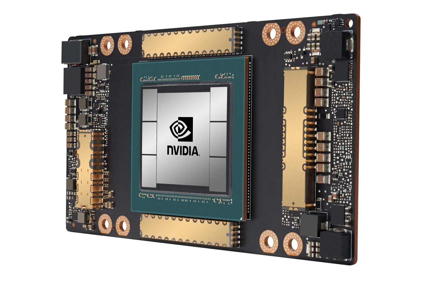
NVIDIA CEO Jensen Huang in a pre-GTC press briefing stressed that the upcoming "Ampere" graphics architecture will spread across both the company's compute-accelerator and commercial graphics product lines. The architecture makes its debut later today with the Tesla A100 HPC processor for breakthrough AI acceleration. It's unlikely that any GeForce products will be formally announced this month, with rumors pointing to a GeForce "Ampere" product launch at a gaming-focused event in September, close to "Cyberpunk 2077" launch.

It was earlier believed that NVIDIA had forked its breadwinning IP into two lines, one focused on headless scalar compute, and the other on graphics products through the company's GeForce and Quadro product lines. To that effect, its "Volta" architecture focused on scalar-compute (with the exception of the forgotten TITAN V); and the "Turing" architecture focused solely on GeForce and Quadro. It was then believed that "Ampere" will focus on compute, and the so-called "Hopper" would be this generation's graphics-focused architecture. We now know that won't be the case. We've compiled a selection of GeForce Ampere rumors in this article.


View at TechPowerUp Main Site
 
Interesting, so the GA100 reveal should at least shed a bit more light on what we can expect with the upcoming GA102 and GA104.

And the apparent 7nm die size limitation has already been put to bed.
 
And the apparent 7nm die size limitation has already been put to bed.
The limitation these dies are flirting with is the reticle limit and has been for several generations now. There are practical considerations for die size - yield and price - but for something that sells for $10k, these considerations are greatly reduced.
 
Are there any Die size density numbers for A100. There is some 38000mtr in the database. 54000mtr seems impossible with 858mm 7nm at 46mtrmm. Unless it reached 62mtrmm in which case looks much better than AMDs 41mtrmm chips.
With a standard 6” photomask, on the standard 0.33 NA machine, you get 4x/4x reticle which means a full field of 33 mm by 26 mm for a maximum die size of 858 mm². With 0.55 NA with anamorphic optics, you are looking at 8x in the y-direction, so your field is now halved. For circuit designers, this means an effective field of 16.5 mm by 26 mm for a new maximum die size of 429 mm². Say goodbye to the massive dies we got used to from Intel and Nvidia.
 
Last edited:
Who told them my bday is in September? On top of it they want to tie it with Cyberpunk launch? Bastards!
 
And the apparent 7nm die size limitation has already been put to bed.

There are 3 different N7 processes - TSMC N7FF | TSMC N7P (2nd gen N7FF) | TSMC N7FF+.

AMD has built four dies - chiplet 74 sq. mm, Navi 10 251 sq. mm, Vega 20 that is 331 sq. mm and Renoir that is 156 sq. mm (62.82 MTr/sq. mm).

It is quite possible that the first iteration of the N7 process, namely the TSMC N7FF has indeed a limitation up to 429 sq. mm.

Otherwise, why is Nvidia is late if not to wait the next processes ?


Are there any Die size density numbers for A100. There is some 38000mtr in the database. 54000mtr seems impossible with 858mm 7nm at 46mtrmm. Unless it reached 62mtrmm in which case looks much better than AMDs 41mtrmm chips.


65.37 MTr/ sq. mm if 54B and 826.
 
Last edited:
AMD has built four dies - chiplet 74 sq. mm, Navi 10 251 sq. mm, Vega 20 that is 331 sq. mm and Renoir that is 156 sq. mm (62.82 MTr/sq. mm).
It is quite possible that the first iteration of the N7 process, namely the TSMC N7FF has indeed a limitation up to 429 sq. mm.
99% sure this is not the case. Reticle size has not changed and definitely not by that much. All the dies you listed are for either consumer or comparatively lower-margin products. Yield and cost issues prevent making bigger ones. 7N processes are also much more mature now than they were when AMD came out with most of the listed stuff.
 
99% sure this is not the case. Reticle size has not changed and definitely not by that much. All the dies you listed are for either consumer or comparatively lower-margin products. Yield and cost issues prevent making bigger ones. 7N processes are also much more mature now than they were when AMD came out with most of the listed stuff.

AMD had never built so small dies on average before the N7 process, remember the Vega 10 on 14nm or Fiji on 28nm ?

What cost do you mean - the one that is always transfered to the buyers? How much does the RX 5700 cost and does AMD have competition to Nvidia's RTX 2080, RTX 2080 S, RTX 2080 Ti, RTX Titan and Volta ? No!
 
It was earlier believed that NVIDIA had forked its breadwinning IP into two lines, one focused on headless scalar compute, and the other on graphics products through the company's GeForce and Quadro product lines.

That was a gross misunderstanding. Mr Hwang publicly stated Volta won't come to the consumer space simply because it was too complex.
Lo and behold, a couple of years later Turing was still about big, expensive dies. And that was the first time Nvidia did that (that I can recall), they have never hinted at splitting their architectures. In fact, if you look at their MO, they're optimizing costs by unifying everything that makes sense to be unified.
 
AMD had never built so small dies on average before the N7 process, remember the Vega 10 on 14nm or Fiji on 28nm ?
Remember Evergreen on 40nm? 334mm2 for the flagship GPU compared to the GTX 480's 529mm2.

"AMD had never built so small dies on average" Cmon now, remember your history lessons. AMD's entire marketing push for the HD 3000/4000/5000/6000 series was "small efficient dies".
 
Back then they had X2 cards.
And also, that was after the R600 disaster and they were scared to build larger dies, Fiji is 596 sq. mm!
What do X2 cards have to do with anything?

You stated that AMD had never built a line of small dies, I showed you that was factually incorrect. AMD has done this higher density smaller die strategy before, this is nothing new.
 
What do X2 cards have to do with anything?

You stated that AMD had never built a line of small dies, I showed you that was factually incorrect. AMD has done this higher density smaller die strategy before, this is nothing new.

You are factually incorrect claiming that Radeon HD 5870 was a flagship, then Radeon HD 5970 was the flagship, as well as Radeon HD 6990 and Radeon HD 7990 all which were 2-GPU cards.
It has to do that AMD had never abandoned the enthusiasts segment before the N7 process.
 
Low quality post by bug
0gKRkoK.gif


:)
That didn't go well for "Johnny" after all :P
 
Turing was Volta with RT cores, so next gen geforce will be Ampere with RT again, and some tensor, int and fp rebalance for graphics.
 
So as I expected no Geforce news until the September paper launch.
 
Back
Top