- Joined
- Oct 9, 2007
- Messages
- 47,511 (7.49/day)
- Location
- Hyderabad, India
| System Name | RBMK-1000 |
|---|---|
| Processor | AMD Ryzen 7 5700G |
| Motherboard | ASUS ROG Strix B450-E Gaming |
| Cooling | DeepCool Gammax L240 V2 |
| Memory | 2x 8GB G.Skill Sniper X |
| Video Card(s) | Palit GeForce RTX 2080 SUPER GameRock |
| Storage | Western Digital Black NVMe 512GB |
| Display(s) | BenQ 1440p 60 Hz 27-inch |
| Case | Corsair Carbide 100R |
| Audio Device(s) | ASUS SupremeFX S1220A |
| Power Supply | Cooler Master MWE Gold 650W |
| Mouse | ASUS ROG Strix Impact |
| Keyboard | Gamdias Hermes E2 |
| Software | Windows 11 Pro |
A lot is riding for Intel on its 11th Gen Core "Tiger Lake" system-on-chip (SoC), which will launch exclusively on mobile platforms, hoping to dominate the 7 W thru 15 W ultraportable form-factors in 2020, while eventually scaling up to the 25 W thru 45 W H-segment form-factors in 2021, with a variant that is rumored to double core-counts. The chip is built on Intel's new 10 nm SuperFin silicon fabrication node that enables a double digit percentage energy efficiency growth over 10 nm, allowing Intel to significantly dial up clock speeds without impacting the power envelope. The CPU and iGPU make up the two key components of the "Tiger Lake" SoC.
The CPU component on the "Tiger Lake" processors that launch in a few weeks from now features four "Willow Cove" CPU cores. Coupled with HyperThreading, this ends up being a 4-core/8-thread setup, although much of Intel's innovation is in giving these cores significant IPC increases over the "Skylake" core powering "Comet Lake" processors, and compared to the "Sunny Cove" cores powering "Ice Lake" a minor IPC (although major net performance increase from clock speeds). The "Willow Cove" CPU core appears to be a derivative of the "Sunny Cove" core, designed to take advantage of the 10 nm SuperFin node, along with three key innovations.

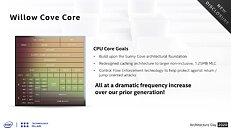

To begin with, "Willow Cove" features a beefed up cache sub-system. While the L1 caches are untouched, the dedicated L2 cache has now increased in size to 1280 KB (1.25 MB), up from 512 KB on the "Sunny Cove" core, and 256 KB on "Skylake." This increase in size is attributable to the non-inclusive nature of the cache, i.e., data can only either reside in this cache, or retire to the last-level L3 cache, but can never exist on both caches at the same time. The last-level L3 cache, shared between the 4 cores on the "Tiger Lake" SoC, too, has been enlarged, and is now 12 MB in size. The L3 cache is non-inclusive, just like the L2c. The "Willow Cove" core also features Control Flow Enforcement technology, which is a hardware-level hardening against return/jump oriented side-channel attacks. Optimized for the 10 nm SuperFin node, "Willow Cove" cores will run at significantly higher clock speeds than "Sunny Cove" cores, resulting in a net performance gain over "Ice Lake" within the same power envelope.
The second key component of "Tiger Lake" is the Gen12 integrated graphics processor built on the Xe LP architecture. Xe is designed to be scalable all the way from tiny iGPUs such as this one, to exa-scale HPC processors under the Xe HP banner. On "Tiger Lake," the Xe LP iGPU promises a 2x performance gain over the Gen11 iGPU inside "Ice Lake." A bulk of the innovation lies with a 50% increase in SIMD muscle (execution units), and a combination of IPC and clock speed increases, coupled with a redesigned cache structure dedicated to the iGPU.


The Xe LP iGPU features 96 execution units - a 50% increase over the previous generation. Intel redesigned the execution unit to make it more efficient, with eight pipelines each that can handle both Float and INT ops concurrently, coupled with two dedicated extended math pipelines. This is loosely analogous to the concurrent FP+INT execution NVIDIA introduced with "Turing" CUDA cores. The 8-wide FP+INT ALUs offer double the INT16 and INT32 execution performance over the previous generation, and introduce INT8 rapid math.
Two Xe LP EUs share a common thread controller, along with software scoreboarding. Each Xe LP sub-slice shares an instruction cache, a thread dispatch controller, L1 texture cache, and samplers, among 16 execution units. The Xe LP iGPU on "Tiger Lake" features six such sub-slices. On the front-end sit geometry (including tessellation), raster, and pixel dispatch components; and on the back-end are three pixel back-ends with 24 ROPs. The iGPU features a dedicated L3 cache of its own. Intel mentions the size of this cache as "up to 16 MB." Although Intel did not mention frequency, it mentioned that the 10 nm SuperFin proces affords Xe LP with up to 70% higher iGPU frequencies at a given iso-voltage than Gen11.
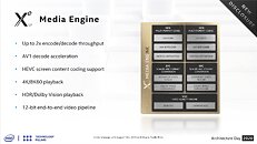
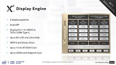
Raw muscle power only paints half the picture, the other half are the media and display capabilities of the Xe LP iGPU. The new Xe LP media engine feature a 2x increase in media encode/decode performance, to double the hardware-acceleration performance over the previous generation, allowing Intel to add support for newer video formats that demand more compute power. This increase stems from the deployment of two sets of independent MPX (multi-format codecs) and scalar format conversion. The new media engine supports AV1 hardware decode, HEVC screen content coding, HDR and Dolby Vision playback acceleration, and a 12 bits per cell end-to-end video pipeline. Video resolutions of up to 8K 60 FPS should run smooth on this iGPU. The display engine of the Xe LP iGPU is easily on par with discrete GPUs from NVIDIA and AMD. It features four display pipelines, supporting dual eDP. Among the display output standards supported are DisplayPort 1.4, HDMI 2.0, Thunderbolt 4, and USB4 type-C. It supports resolutions of up to 8K and various ultra-wide resolutions, along with HDR10 and Dolby Vision, with 12-bpc color formats. Refresh rates of up to 360 Hz, and VESA Adaptive Sync are also supported.
The CPU and iGPU come together on the SoC, which shares various key components between the two, beginning with a dual Ringbus interconnect that offers double the interconnect bandwidth compared to the previous generation. The integrated memory controller of "Tiger Lake" supports up to 128 GB of dual-channel DDR4-3200 (native), LPDDR5-5400, and LPDDR4x. Other key SoC components include FIVR (fully integrated voltage regulation), a unified type-C controller that combines Thunderbolt 4, USB4, and DisplayPort passthrough; and a PCI-Express gen 4.0 root complex that puts out not just 16 lanes toward PEG (discrete graphics), but also 4 lanes toward a CPU-attached M.2 NVMe slot.
View at TechPowerUp Main Site
The CPU component on the "Tiger Lake" processors that launch in a few weeks from now features four "Willow Cove" CPU cores. Coupled with HyperThreading, this ends up being a 4-core/8-thread setup, although much of Intel's innovation is in giving these cores significant IPC increases over the "Skylake" core powering "Comet Lake" processors, and compared to the "Sunny Cove" cores powering "Ice Lake" a minor IPC (although major net performance increase from clock speeds). The "Willow Cove" CPU core appears to be a derivative of the "Sunny Cove" core, designed to take advantage of the 10 nm SuperFin node, along with three key innovations.


To begin with, "Willow Cove" features a beefed up cache sub-system. While the L1 caches are untouched, the dedicated L2 cache has now increased in size to 1280 KB (1.25 MB), up from 512 KB on the "Sunny Cove" core, and 256 KB on "Skylake." This increase in size is attributable to the non-inclusive nature of the cache, i.e., data can only either reside in this cache, or retire to the last-level L3 cache, but can never exist on both caches at the same time. The last-level L3 cache, shared between the 4 cores on the "Tiger Lake" SoC, too, has been enlarged, and is now 12 MB in size. The L3 cache is non-inclusive, just like the L2c. The "Willow Cove" core also features Control Flow Enforcement technology, which is a hardware-level hardening against return/jump oriented side-channel attacks. Optimized for the 10 nm SuperFin node, "Willow Cove" cores will run at significantly higher clock speeds than "Sunny Cove" cores, resulting in a net performance gain over "Ice Lake" within the same power envelope.
The second key component of "Tiger Lake" is the Gen12 integrated graphics processor built on the Xe LP architecture. Xe is designed to be scalable all the way from tiny iGPUs such as this one, to exa-scale HPC processors under the Xe HP banner. On "Tiger Lake," the Xe LP iGPU promises a 2x performance gain over the Gen11 iGPU inside "Ice Lake." A bulk of the innovation lies with a 50% increase in SIMD muscle (execution units), and a combination of IPC and clock speed increases, coupled with a redesigned cache structure dedicated to the iGPU.


The Xe LP iGPU features 96 execution units - a 50% increase over the previous generation. Intel redesigned the execution unit to make it more efficient, with eight pipelines each that can handle both Float and INT ops concurrently, coupled with two dedicated extended math pipelines. This is loosely analogous to the concurrent FP+INT execution NVIDIA introduced with "Turing" CUDA cores. The 8-wide FP+INT ALUs offer double the INT16 and INT32 execution performance over the previous generation, and introduce INT8 rapid math.
Two Xe LP EUs share a common thread controller, along with software scoreboarding. Each Xe LP sub-slice shares an instruction cache, a thread dispatch controller, L1 texture cache, and samplers, among 16 execution units. The Xe LP iGPU on "Tiger Lake" features six such sub-slices. On the front-end sit geometry (including tessellation), raster, and pixel dispatch components; and on the back-end are three pixel back-ends with 24 ROPs. The iGPU features a dedicated L3 cache of its own. Intel mentions the size of this cache as "up to 16 MB." Although Intel did not mention frequency, it mentioned that the 10 nm SuperFin proces affords Xe LP with up to 70% higher iGPU frequencies at a given iso-voltage than Gen11.


Raw muscle power only paints half the picture, the other half are the media and display capabilities of the Xe LP iGPU. The new Xe LP media engine feature a 2x increase in media encode/decode performance, to double the hardware-acceleration performance over the previous generation, allowing Intel to add support for newer video formats that demand more compute power. This increase stems from the deployment of two sets of independent MPX (multi-format codecs) and scalar format conversion. The new media engine supports AV1 hardware decode, HEVC screen content coding, HDR and Dolby Vision playback acceleration, and a 12 bits per cell end-to-end video pipeline. Video resolutions of up to 8K 60 FPS should run smooth on this iGPU. The display engine of the Xe LP iGPU is easily on par with discrete GPUs from NVIDIA and AMD. It features four display pipelines, supporting dual eDP. Among the display output standards supported are DisplayPort 1.4, HDMI 2.0, Thunderbolt 4, and USB4 type-C. It supports resolutions of up to 8K and various ultra-wide resolutions, along with HDR10 and Dolby Vision, with 12-bpc color formats. Refresh rates of up to 360 Hz, and VESA Adaptive Sync are also supported.
The CPU and iGPU come together on the SoC, which shares various key components between the two, beginning with a dual Ringbus interconnect that offers double the interconnect bandwidth compared to the previous generation. The integrated memory controller of "Tiger Lake" supports up to 128 GB of dual-channel DDR4-3200 (native), LPDDR5-5400, and LPDDR4x. Other key SoC components include FIVR (fully integrated voltage regulation), a unified type-C controller that combines Thunderbolt 4, USB4, and DisplayPort passthrough; and a PCI-Express gen 4.0 root complex that puts out not just 16 lanes toward PEG (discrete graphics), but also 4 lanes toward a CPU-attached M.2 NVMe slot.
View at TechPowerUp Main Site

