- Joined
- Oct 9, 2007
- Messages
- 47,379 (7.52/day)
- Location
- Hyderabad, India
| System Name | RBMK-1000 |
|---|---|
| Processor | AMD Ryzen 7 5700G |
| Motherboard | ASUS ROG Strix B450-E Gaming |
| Cooling | DeepCool Gammax L240 V2 |
| Memory | 2x 8GB G.Skill Sniper X |
| Video Card(s) | Palit GeForce RTX 2080 SUPER GameRock |
| Storage | Western Digital Black NVMe 512GB |
| Display(s) | BenQ 1440p 60 Hz 27-inch |
| Case | Corsair Carbide 100R |
| Audio Device(s) | ASUS SupremeFX S1220A |
| Power Supply | Cooler Master MWE Gold 650W |
| Mouse | ASUS ROG Strix Impact |
| Keyboard | Gamdias Hermes E2 |
| Software | Windows 11 Pro |
Intel in the opening presentation of the Hot Chips 32 virtual conference detailed its next-generation Xeon Scalable "Ice Lake-SP" enterprise processor. Built on the company's 10 nm silicon fabrication process, "Ice Lake-SP" sees the first non-client and non-mobile deployment of the company's new "Sunny Cove" CPU core that introduces higher IPC than the "Skylake" core that's been powering Intel microarchitectures since 2015. While the "Sunny Cove" core itself is largely unchanged from its implementation in 10th Gen Core "Ice Lake-U" mobile processors, it conforms to the cache hierarchy and tile silicon topology of Intel's enterprise chips.
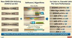
The "Ice Lake-SP" die Intel talked about in its Hot Chips 32 presentation had 28 cores. The "Sunny Cove" CPU core is configured with the same 48 KB L1D cache as its client-segment implementation, but a much larger 1280 KB (1.25 MB) dedicated L2 cache. The core also receives a second fused multiply/add (FMA-512) unit, which the client-segment implementation lacks. It also receives a handful new instruction sets exclusive to the enterprise segment, including AVX-512 VPMADD52, Vector-AES, Vector Carry-less Multiply, GFNI, SHA-NI, Vector POPCNT, Bit Shuffle, and Vector BMI. In one of the slides, Intel also detailed the performance uplifts from the new instructions compared to "Cascade Lake-SP".


Besides higher IPC from the "Sunny Cove" cores, an equally big selling point for "Ice Lake-SP" is its improved and modernized I/O. To begin with, the processor comes with an 8-channel DDR4 interface for the 28-core die. This is accomplished using four independent memory controller tiles, each with two memory channels. The previous-generation 28-core "Cascade Lake-SP" die features two memory controller tiles, each with three memory channels, making up its 6-channel interface. Each of the memory controllers features fixed-function hardware for total memory encryption using the AES-XTS 128-bit algorithm without CPU overhead. Improvements were also made to the per-channel scheduling.


Besides the 8-channel memory interface, the other big I/O feature is PCI-Express gen 4.0 bus. The 28-core "Ice Lake-SP" die features four independent PCIe Gen4 root-complex tiles. Intel enabled all enterprise-relevant features of PCIe Gen4, including I/O virtualization, and a P2P credit fabric to improve P2P bandwidth. The "Ice Lake-SP" silicon is also ready for Intel's Optane Persistent Memory 200 "Barlow Pass" series. The die also features three UPI links for inter-socket or inter-die communication, put out by independent UPI controllers that have their own mesh interconnect ring stops.


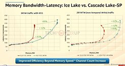
The main interconnect on the "Ice Lake-SP" die is a refined second-generation mesh interconnect, which coupled with the improved floor-planning and new features, works to significantly reduce interconnect-level latencies over the previous generation dies. Intel also worked to improve memory access and latencies beyond simply dialing up memory channels and frequency.

Besides benefiting from the switch to the 10 nm silicon fabrication process, "Ice Lake-SP" introduces several new power management latency reduction features, including Fast Core Frequency Change, and Coherent Mesh Fabric Drainless Frequency Change. Effort also appears to be put in the area of improving CPU core frequencies in response to AVX-512 workloads.

Intel Speed Select Technology is a unique new feature that allows admins to power-gate CPU cores to spend the processor's TDP budget to bump up frequency on fewer cores. This allows you to reconfigure the 28-core die to something like a 16-core or even 8-core die, on the fly, with aggressive clock speed profile. This feature is also used to power-gate cores when not needed, to minimize the server's power draw.

Intel is expected to launch its Xeon Scalable "Ice Lake-SP" processor within 2H-2020.
View at TechPowerUp Main Site
The "Ice Lake-SP" die Intel talked about in its Hot Chips 32 presentation had 28 cores. The "Sunny Cove" CPU core is configured with the same 48 KB L1D cache as its client-segment implementation, but a much larger 1280 KB (1.25 MB) dedicated L2 cache. The core also receives a second fused multiply/add (FMA-512) unit, which the client-segment implementation lacks. It also receives a handful new instruction sets exclusive to the enterprise segment, including AVX-512 VPMADD52, Vector-AES, Vector Carry-less Multiply, GFNI, SHA-NI, Vector POPCNT, Bit Shuffle, and Vector BMI. In one of the slides, Intel also detailed the performance uplifts from the new instructions compared to "Cascade Lake-SP".


Besides higher IPC from the "Sunny Cove" cores, an equally big selling point for "Ice Lake-SP" is its improved and modernized I/O. To begin with, the processor comes with an 8-channel DDR4 interface for the 28-core die. This is accomplished using four independent memory controller tiles, each with two memory channels. The previous-generation 28-core "Cascade Lake-SP" die features two memory controller tiles, each with three memory channels, making up its 6-channel interface. Each of the memory controllers features fixed-function hardware for total memory encryption using the AES-XTS 128-bit algorithm without CPU overhead. Improvements were also made to the per-channel scheduling.


Besides the 8-channel memory interface, the other big I/O feature is PCI-Express gen 4.0 bus. The 28-core "Ice Lake-SP" die features four independent PCIe Gen4 root-complex tiles. Intel enabled all enterprise-relevant features of PCIe Gen4, including I/O virtualization, and a P2P credit fabric to improve P2P bandwidth. The "Ice Lake-SP" silicon is also ready for Intel's Optane Persistent Memory 200 "Barlow Pass" series. The die also features three UPI links for inter-socket or inter-die communication, put out by independent UPI controllers that have their own mesh interconnect ring stops.


The main interconnect on the "Ice Lake-SP" die is a refined second-generation mesh interconnect, which coupled with the improved floor-planning and new features, works to significantly reduce interconnect-level latencies over the previous generation dies. Intel also worked to improve memory access and latencies beyond simply dialing up memory channels and frequency.

Besides benefiting from the switch to the 10 nm silicon fabrication process, "Ice Lake-SP" introduces several new power management latency reduction features, including Fast Core Frequency Change, and Coherent Mesh Fabric Drainless Frequency Change. Effort also appears to be put in the area of improving CPU core frequencies in response to AVX-512 workloads.

Intel Speed Select Technology is a unique new feature that allows admins to power-gate CPU cores to spend the processor's TDP budget to bump up frequency on fewer cores. This allows you to reconfigure the 28-core die to something like a 16-core or even 8-core die, on the fly, with aggressive clock speed profile. This feature is also used to power-gate cores when not needed, to minimize the server's power draw.

Intel is expected to launch its Xeon Scalable "Ice Lake-SP" processor within 2H-2020.
View at TechPowerUp Main Site


