- Joined
- Aug 19, 2017
- Messages
- 3,233 (1.12/day)
Currently, Intel's best silicon manufacturing process available to desktop users is their 14 nm node, specifically the 14 nm+++ variant, which features several enhancements so it can achieve a higher frequencies and allow for faster gate switching. Compare that to AMD's best, a Ryzen 3000 series processor based on Zen 2 architecture, which is built on TSMC's 7 nm node, and you would think AMD is in clear advantage there. Well, it only sort of is. German hardware overclocker and hacker, der8auer, has decided to see how one production level silicon compares to another, and he put it to the test. He decided to use Intel's Core i9-10900K processor and compare it to AMD's Ryzen 9 3950X under a scanning electron microscope (SEM).
First, der8auer took both chips and detached them from their packages; then he proceeded to grind them as much as possible so SEM could do its job of imaging the chips sans the substrate and protective barrier. This was followed by securing the chips to a sample holder using an electrically conductive adhesive to improve penetration of the high energy electrons from the SEM electron gun. To get as fair a comparison as possible, he used the L2 cache component of both processors as they are usually the best representatives of a node. This happens because the logic portion of the chip differs according to architecture; hence, level two cache is used to get a fair comparison - it's design is much more standardized.
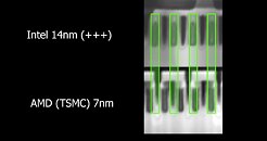
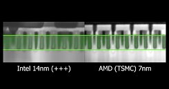
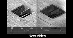
The results? Well, the Intel 14 nm chip features transistors with a gate width of 24 nm, while the AMD/TSMC 7 nm one has a gate width of 22 nm (gate height is also rather similar). While these are not much different, TSMC's node is still much denser compared to Intel's - TSMC's 7 nm produces chips with a transistor density around 90 MT/mm² (million transistors per square millimeter), which is comparable in density to Intel's 10 nm node used on recent mobile processors. Below you can see the SEM images and comparison made. For more information and details please head over to the source.
Another interesting thing to note here, the gate width is not following the naming scheme as you might have expected. The 14 nm transistor isn't 14 nm in width, and the 7 nm transistor isn't 7 nm wide. The naming of the node and actual size of the node have had a departure a long time ago, and the naming convention is really up to the manufacturer - it's become more of a marketing gimmick than anything else. This is the reason researchers have already proposed another density metric for semiconductor technology other than pure "nm" terms.
View at TechPowerUp Main Site
First, der8auer took both chips and detached them from their packages; then he proceeded to grind them as much as possible so SEM could do its job of imaging the chips sans the substrate and protective barrier. This was followed by securing the chips to a sample holder using an electrically conductive adhesive to improve penetration of the high energy electrons from the SEM electron gun. To get as fair a comparison as possible, he used the L2 cache component of both processors as they are usually the best representatives of a node. This happens because the logic portion of the chip differs according to architecture; hence, level two cache is used to get a fair comparison - it's design is much more standardized.


The results? Well, the Intel 14 nm chip features transistors with a gate width of 24 nm, while the AMD/TSMC 7 nm one has a gate width of 22 nm (gate height is also rather similar). While these are not much different, TSMC's node is still much denser compared to Intel's - TSMC's 7 nm produces chips with a transistor density around 90 MT/mm² (million transistors per square millimeter), which is comparable in density to Intel's 10 nm node used on recent mobile processors. Below you can see the SEM images and comparison made. For more information and details please head over to the source.
Another interesting thing to note here, the gate width is not following the naming scheme as you might have expected. The 14 nm transistor isn't 14 nm in width, and the 7 nm transistor isn't 7 nm wide. The naming of the node and actual size of the node have had a departure a long time ago, and the naming convention is really up to the manufacturer - it's become more of a marketing gimmick than anything else. This is the reason researchers have already proposed another density metric for semiconductor technology other than pure "nm" terms.
View at TechPowerUp Main Site


