- Joined
- Aug 19, 2017
- Messages
- 2,651 (0.99/day)
Apple has established itself as a master of silicon integrated circuit design and has proven over the years that its processors deliver the best results, generation after generation. If we take a look at the performance numbers of the latest A14 Bionic, you can conclude that its performance is now rivaling some of the x86_64 chips. So you would wonder, what is inside this SoC that makes it so fast? That is exactly what ICmasters, a semiconductor reverse engineering and IP services company, has questioned and decided to find out. For starters, we know that Apple manufactures the new SoCs on TSMC's N5 5 nm node. The Taiwanese company promises to pack 171.3 million transistors per square millimeter, so how does it compare to an actual product?
ICmasters have used electron microscopy to see what the chip is made out of and to measure the transistor density. According to this source, Apple has a chip with a die size of 88 mm², which packs 11.8 billion N5 transistors. The density metric, however, doesn't correspond to that of TSMC. Instead of 171.3 million transistors per mm², the ICmasters measured 134.09 million transistors per mm². This is quite a difference, however, it is worth noting that each design will have it different due to different logic and cache layout.


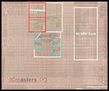
The SoC packs a 16-core neural engine, quad-cluster GPU, and six general-purpose cores, two of which are high-performance "big" FireStorm cores, while the remaining six are more efficient "LITTLE" IceStorm designs. If we break down the die usage of these cores, we can see that FireStorm cores with a big level two (L2) cache use about 9.1 mm² of the die, while the four IceStorm cores with small L2 cache use 6.44 mm². The GPU cluster is using about 11.65 mm² sizes of the portion. There is a unified system cache present on the die, however, it is a bit hard to find.
View at TechPowerUp Main Site
ICmasters have used electron microscopy to see what the chip is made out of and to measure the transistor density. According to this source, Apple has a chip with a die size of 88 mm², which packs 11.8 billion N5 transistors. The density metric, however, doesn't correspond to that of TSMC. Instead of 171.3 million transistors per mm², the ICmasters measured 134.09 million transistors per mm². This is quite a difference, however, it is worth noting that each design will have it different due to different logic and cache layout.


The SoC packs a 16-core neural engine, quad-cluster GPU, and six general-purpose cores, two of which are high-performance "big" FireStorm cores, while the remaining six are more efficient "LITTLE" IceStorm designs. If we break down the die usage of these cores, we can see that FireStorm cores with a big level two (L2) cache use about 9.1 mm² of the die, while the four IceStorm cores with small L2 cache use 6.44 mm². The GPU cluster is using about 11.65 mm² sizes of the portion. There is a unified system cache present on the die, however, it is a bit hard to find.
View at TechPowerUp Main Site


