Raevenlord
News Editor
- Joined
- Aug 12, 2016
- Messages
- 3,755 (1.20/day)
- Location
- Portugal
| System Name | The Ryzening |
|---|---|
| Processor | AMD Ryzen 9 5900X |
| Motherboard | MSI X570 MAG TOMAHAWK |
| Cooling | Lian Li Galahad 360mm AIO |
| Memory | 32 GB G.Skill Trident Z F4-3733 (4x 8 GB) |
| Video Card(s) | Gigabyte RTX 3070 Ti |
| Storage | Boot: Transcend MTE220S 2TB, Kintson A2000 1TB, Seagate Firewolf Pro 14 TB |
| Display(s) | Acer Nitro VG270UP (1440p 144 Hz IPS) |
| Case | Lian Li O11DX Dynamic White |
| Audio Device(s) | iFi Audio Zen DAC |
| Power Supply | Seasonic Focus+ 750 W |
| Mouse | Cooler Master Masterkeys Lite L |
| Keyboard | Cooler Master Masterkeys Lite L |
| Software | Windows 10 x64 |
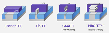
The Taiwan Economic Daily claims that TSMC has achieved a major internal breakthrough for the eventual rollout of 2 nm fabrication process technology. According to the publication, this breakthrough has turned TSMC even more optimistic towards a 2023 rollout of 2 nm risk production - which is all the more impressive considering reports that TSMC will be leaving the FinFet realm for a new multi-bridge channel field effect transistor (MBCFET) architecture - itself based on the Gate-All-Around (GAA) technology. This breakthrough comes one year after TSMC put together an internal team whose aim was to pave the way for 2 nm deployment.
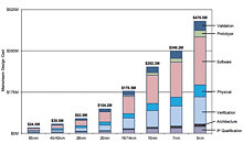
MBCFET expands on the GAAFET architecture by taking the Nanowire field-effect transistor and expanding it so that it becomes a Nanosheet. The main idea is to make the field-effect transistor three-dimensional. This new complementary metal oxide semiconductor transistor can improve circuit control and reduce leakage current. This design philosophy is not exclusive to TSMC - Samsung has plans to deploy a variant of this design on their 3 nm process technology. And as has been the norm, further reductions in chip fabrication scale come at hefty costs - while the development cost for 5 nm has already achieved $476M in cost, Samsung reports that their 3 nm GAA technology will cost in excess of $500M - and 2 nm, naturally, will come in even costlier than that.


View at TechPowerUp Main Site


")


